
Optical receiver method and apparatus

a receiver and optical technology, applied in the field of fiber optical communication systems and techniques, can solve the problems of not being able to singulate into a size as small as a ceramic, unable to achieve the conductor width, warpage issues, etc., and achieve the effect of shortening the path length, reducing inductance, and high frequency operation

Inactive Publication Date: 2016-08-30
QUANTUM ELECTRO OPTO SYST
View PDF13 Cites 0 Cited by
  • Summary
  • Abstract
  • Description
  • Claims
  • Application Information

AI Technical Summary

Benefits of technology

[0014]An advantage of an embodiment of the invention is the support for high frequency operation, thanks to the shorter conductive path that interconnect the photodiode on the top plane to the TIA and circuitry at the opposite side of the bottom plane through the metallized vias and conductive segments. This shorter path length between photodiode and TIA reduces the inductance and thus enhances the bandwidth of the receiver.
[0015]Another advantage involves the design split between the low precision and high precision placement of components onto bottom and top planes, respectively. Low precision placement involving TIA and passive components is done on the bottom plane whereas high precision placement involving photodiode to fiber receptacle alignment is done on the top plane. The method hereof releases the capacity of the high precision placement machine from low precision placement steps, thus increasing the throughput (and reducing cost) of the high precision placement equipment.
[0016]Also, components interconnected vertically between top plane and bottom plane save substantially the area per unit substrate in the horizontal plane and increase the area available for other components.
[0017]In one disclosed embodiment, the area per unit substrate is shrunk down further by incorporating slot openings on the cavity sidewall shelf for wire bonding directly to conductive pads on slot surfaces from the TIA. As will be described, this serves to reduce the length of conductive paths at the bottom plane from components to the third surface.

Problems solved by technology

However, the metallization on PCB is not able to achieve the conductor width, conductor pitch and pad dimension as small as can be achieved with ceramic.
Furthermore, PCB has warpage issues and is not as flat as ceramic panel.
Moreover, PCB cannot be singulated into a size as small as a ceramic.

Method used


Image

  • Optical receiver method and apparatus
  • Optical receiver method and apparatus
  • Optical receiver method and apparatus

Examples


Embodiment Construction

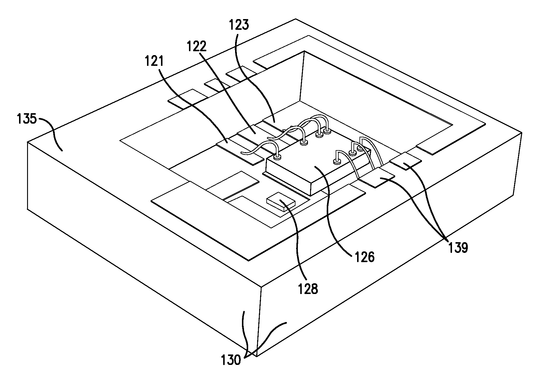
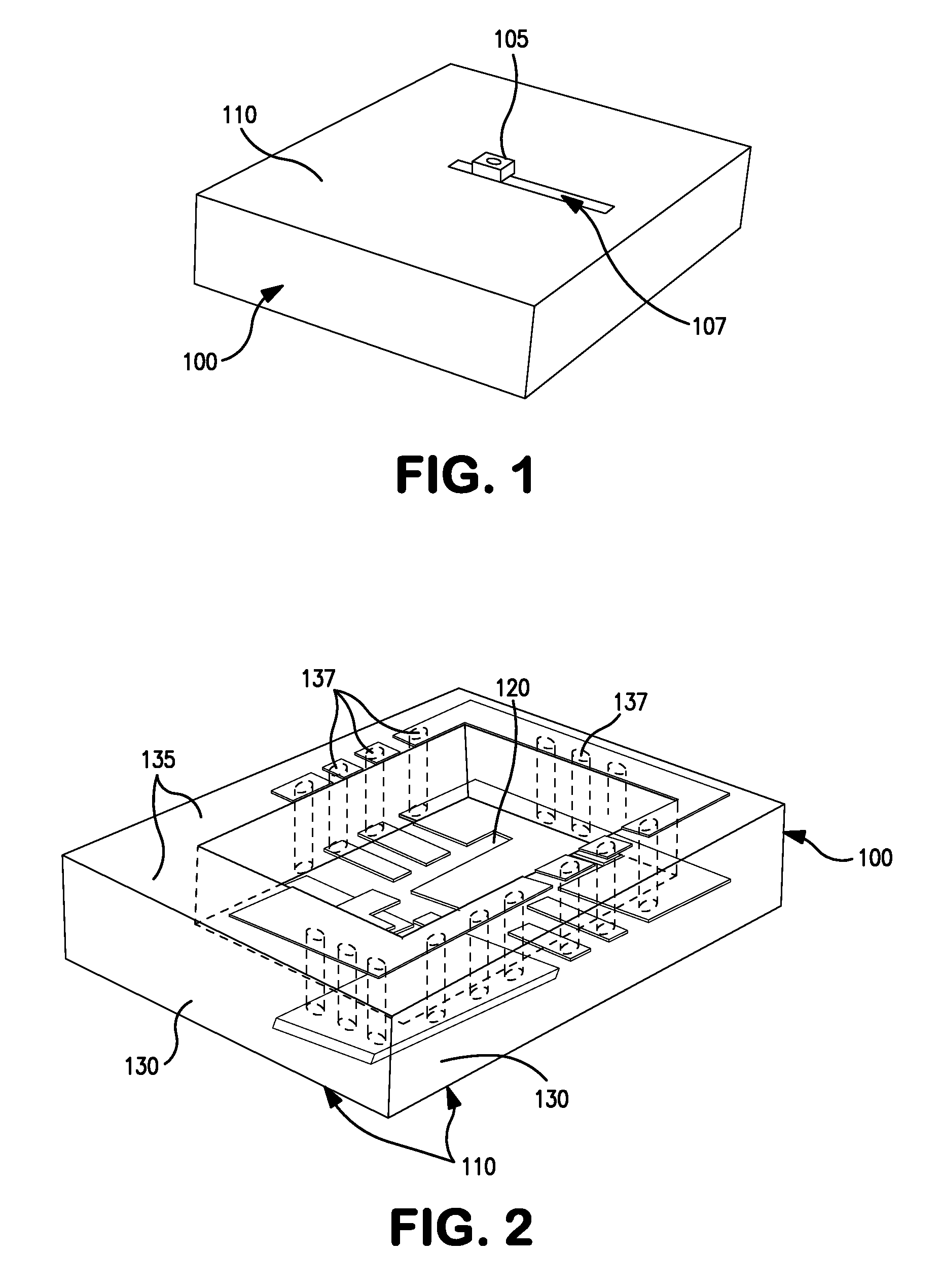
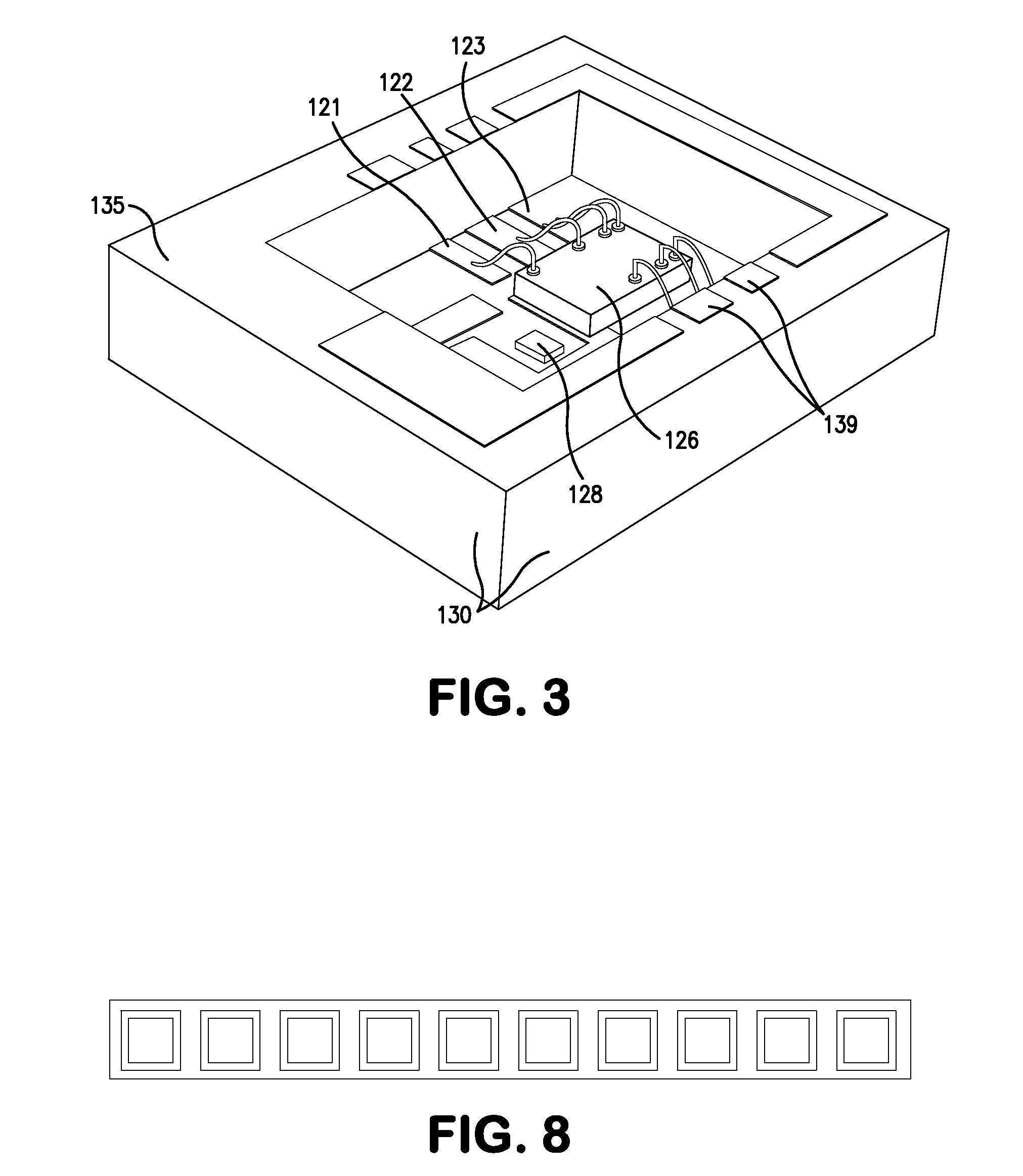
[0027]FIGS. 1 and 2 show an embodiment of an optical receiver apparatus in accordance with an embodiment of the invention and which is illustrative of an embodiment of the method of the invention. An open-ended cavity 100, is formed of an insulating material such as a ceramic. In the illustrated embodiment, the outer locus of the cavity is generally in the shape of a three-dimensional parallelepiped and includes a base having an outside surface 110, an inside surface 120, and peripheral sidewalls represented at 130. At the open end of the cavity, the sidewalls 130 terminate at a planar sidewall shelf 135.

[0028]In the present embodiment, there are three planes on which conductive metallization regions (which may be strips or segments thereof) are applied. For reference, the outside surface 110 of the base is referred to as the “first surface”, and it defines one of the planes which is called the top plane. The inside surface of the base is referred to as the “second surface”, and it ...


PUM

PropertyMeasurementUnit
conductiveaaaaaaaaaa
thicknessaaaaaaaaaa
speedaaaaaaaaaa

Abstract

A method for making an optical receiver assembly that can receive optical signals via an input optical fiber and can generate output electrical signals, including the following steps: providing an open-ended cavity formed of insulating material, such as a ceramic, comprising a base, peripheral sidewalls, and an open end opposite the base, the outside surface of the base defining a first surface and the inside surface of the base defining a second surface; disposing a first conductive region on a portion of the first surface and a second conductive region on a portion of the second surface; mounting, on the first surface, a semiconductor photodetector device having an active region for communicating optically with the input optical fiber, and coupling an electrical output of the photodetector device with the first conductive region; mounting, on the second surface, an amplifier that is electrically coupled with the second conductive region and produces the output electrical signals; and providing at least one conductive via through the thickness of the base and between the first and second conductive regions for coupling the electrical output of the photodetector device with the amplifier.

Description

PRIORITY CLAIM[0001]Priority is claimed from U.S. Provisional Patent Application No. 61 / 956,046, filed May 30, 2013, and said Provisional Patent Application is incorporated herein by reference.FIELD OF THE INVENTION[0002]This invention relates to the field of fiber optical communication systems and techniques and, more particularly, to an optical receiver apparatus and method that has attributes of improved manufacturability and operation.BACKGROUND OF THE INVENTION[0003]Fiber optical communication systems are in widespread use, and it is important that such systems have optical receiver subsystems that can be manufactured efficiently and inexpensively, and which do not compromise the high speed capability of the communication system.[0004]One aspect of optical receiver design involves minimizing parasitic inductance that arises, in high frequency operation, when conductor length (such as circuit wiring) is relatively long. To control parasitic inductance, the length of electrical c...

Claims


Application Information

Patent Timeline
Patent Type & Authority Patents(United States)
IPC IPC(8): G02B6/36H01L31/18G02B6/42H01L31/0203
CPCG02B6/4295H01L31/0203H01L31/18G02B6/423G02B6/4274G02B6/4292Y10T29/41H01L2224/48465H01L2224/48227H01L2924/00
Inventor CHIN, TEYO TUANWALTER, GABRIEL
Owner QUANTUM ELECTRO OPTO SYST
Learn More