Light emitting device and method of manufacturing the same

a technology of light emitting devices and manufacturing methods, which is applied in the direction of semiconductor devices, basic electric elements, electrical apparatus, etc., can solve the problems of reducing the size of the space formed between the face-down mounted light emitting element and the support member is rather small, and the light extracting efficiency of the light emitting device can be reduced. , the area of the light extracting surface of the light emitting element can be increased, and the effect o

Active Publication Date: 2016-08-09
NICHIA CORP
View PDF47 Cites 2 Cited by
  • Summary
  • Abstract
  • Description
  • Claims
  • Application Information

AI Technical Summary

Benefits of technology

[0020]According to the present invention, in the step of supplying an underfill material by dripping, instead of bringing a dispenser as close as possible to a surface of a light emitting element to supply an underfill material from the dispenser, the underfill material can be injected into an underfill arranging portion which is spaced apart from a side surface of a light emitting element. That is, the underfill is not needed to be in direct contact with a side surface of the light emitting element. Thus, not only accidental adherence of the underfill material to the upper surface of the light emitting element can be prevented but also an excess amount of the underfill material can be held at a portion spaced apart from the side surface of the light emitting element without covering the side surface of the light emitting element. Accordingly, the area of the light extracting surface of the light emitting element can be increased, which allows a reduction in the loss of the output from the light emitting element, and thus the light extracting efficiency of the light emitting device can be improved.
[0021]Further, in the present invention, the underfill arranging portions for injecting the underfill material may be provided by alternating the arranging pattern of the electrically conductive wires which had been formerly disposed on the support member. Accordingly, other materials and a step for forming such specified portions can be omitted, and formation of the portions to be injected with the underfill can be facilitated easily by altering the arranging pattern of the electrically conductive wires.
[0022]Moreover, with the use of the arrangement pattern of the electrically conductive wires which had been formerly disposed on the support member, a wirings pattern which allows obtaining of so-called self-alignment effect can be formed by using portions of the wirings pattern at positions for injecting the underfill material. That is, at the time of connecting the electrodes of the light emitting element by respective electrically conductive members, through the use of the fluidity of the melted electrically conductive member, a wirings pattern can be obtained, along which the light emitting element orients.

Problems solved by technology

In particular, electric components are required for maintaining performance for a long period of time even under severe environment.
Further, the return light may be absorbed by the electrodes or the like, which may result in a decrease in the light extracting efficiency of the light emitting device.
Thus, covering the side surfaces of the light emitting element with the underfill material would result in a decrease in the light extracting efficiency of the light emitting device.
In addition, the sizes of the space formed between the face-down mounted light emitting element and the support member are rather small due to existence of a plural kinds of electrically conductive members between those, which require a very small amount of the underfill material to be supplied to fill the space.
Thus, in view of the workability in the coating step of applying the underfill material, application of an appropriate amount of the underfill which does not cover the side surfaces of the light emitting element is practically difficult to perform.

Method used


Image

  • Light emitting device and method of manufacturing the same
  • Light emitting device and method of manufacturing the same
  • Light emitting device and method of manufacturing the same

Examples


example 1

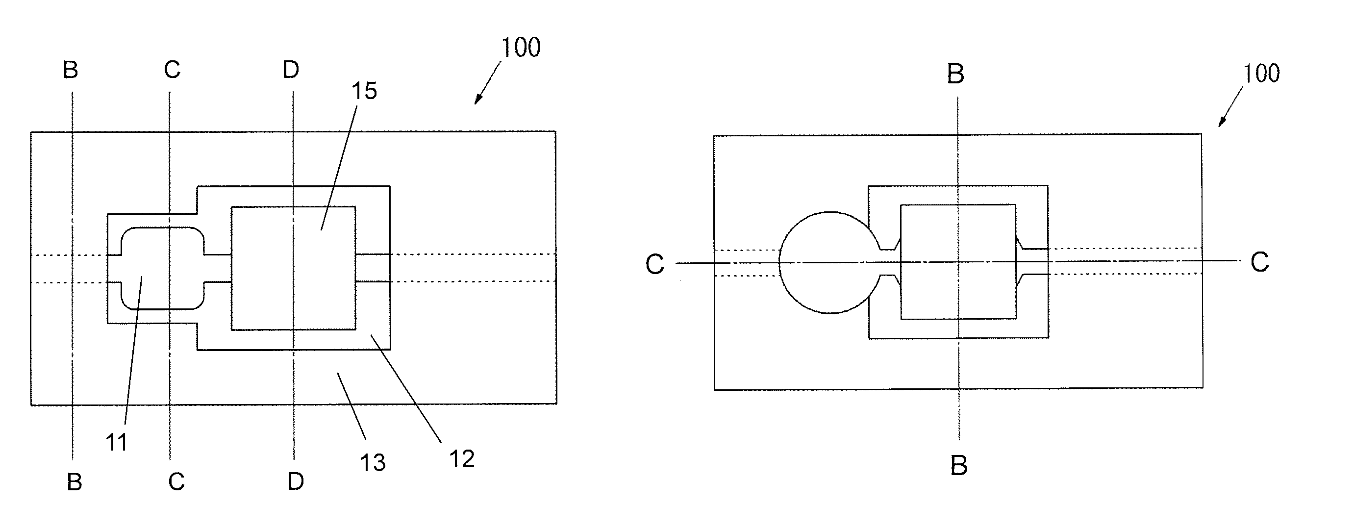
[0085]FIG. 1A is a top view showing a support member of a light emitting device according to the present embodiment. FIGS. 1B, 1C, and 1D are respectively cross-sectional views taken along lines B-B, C-C, and D-D shown in the top view of FIG. 1A respectively.

[0086]As shown in FIGS. 1A to 1D, the support member of the present example includes an underfill arranging portion 17 in a part of a pattern of a pair of positive and negative electrically conductive wirings disposed on the support member. More specifically, on a polyimide film having a thickness of 25 μm which is an insulating member constituting the support member, a copper foil having a thickness of 35 μm is adhered by using an adhesive agent, then, portions of the surface of the adhesive agent or the insulating member so that the copper foil becomes the electrically conductive wirings having a predetermined pattern, and thus the insulating separation portion which includes the underfill wirings portions 17 is formed. Then, ...

example 2

[0092]FIG. 5 is a top view showing a support member of a light emitting device according to the present embodiment. The light emitting device is fabricated in a similar manner as in Example 1, except for that to be described below. The electrically conductive wirings 112 according to the present example includes a protruded portion 112a having a width which is approximately the same as the width of the light emitting element, and the underfill arranging portion is provided adjacent to the protruded portion. That is, as shown in FIG. 5, in the present example, a part of each of the pair of positive and negative electrodes disposed on the support member is formed with a protruded portion having a width approximately the same as the width of the corresponding electrode of the light emitting element 15. In the protruded portions 112a, invisible portions which are hidden behind the light emitting element 15 are shown in dotted lines in FIG. 5. Then, the underfill arranging portion 117 is...


PUM


Abstract

A light emitting device includes a support member, a light emitting element, and an underfill material. The support member includes an insulating member and positive and negative electrically conductive wirings arranged on the insulating member. The electrically conductive wirings are insulated and separated from each other by an insulating region arranged between the positive and negative electrically conductive wirings. The insulating separation region includes a first region disposed on an outer side with respect to the light emitting element and a second region disposed directly under the light emitting element. The first region includes an underfill arranging portion in which an interval between the electrically conductive wirings is wider than in the second region. The underfill material is arranged to extend from the underfill arranging portion to the second region in a space formed between the support member and the light emitting element.

Description

CROSS-REFERENCE TO RELATED APPLICATIONS[0001]This application claims priority to Japanese Patent Application No. 2012-160183 filed on Jul. 19, 2012. The entire disclosure of Japanese Patent Application No. 2009-134281 is hereby incorporated herein by reference.BACKGROUND OF THE INVENTION[0002]1. Field of the Invention[0003]The present invention relates to a light emitting device usable for indicators, lighting apparatuses, displays, backlight of liquid crystal displays, and the like, and a method of manufacturing the same.[0004]2. Discussion of the Related Art[0005]In recent years, various electronic components have been proposed and are put in practical use, and increasingly high performance has been required on such components. In particular, electric components are required for maintaining performance for a long period of time even under severe environment. Light emitting devices employing a semiconductor light emitting element such as a light emitting diode (LED) are no exceptio...

Claims


Application Information

Patent Timeline
Patent Type & Authority Patents(United States)
IPC IPC(8): H01L33/52H01L33/62H01L33/38
CPCH01L33/52H01L33/62H01L33/38H01L2933/0066H01L2224/13H01L2224/73204H01L2933/005
Inventor YAMADA, MOTOKAZU
Owner NICHIA CORP
Why Eureka
Try Eureka