
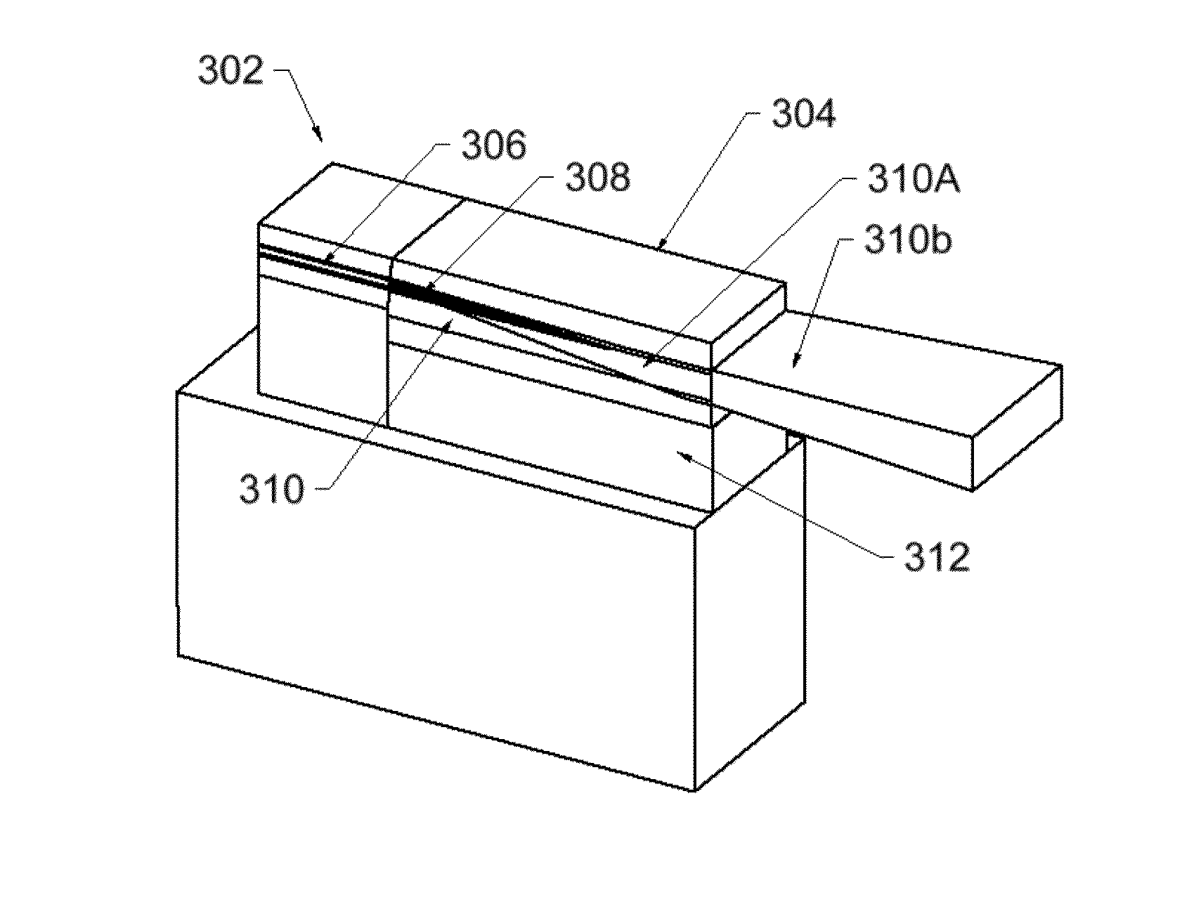
Adiabatic planar waveguide coupler transformer

a technology of planar waveguide coupler and coupler, which is applied in the direction of instruments, mechanical devices, optical elements, etc., can solve the problems of insufficient efficiency of light coupling between light emitted or received by high index and high numerical aperture devices, laser diodes, emitting diodes, etc., and achieve the effect of better material production

Active Publication Date: 2016-06-14
DEMARAY
View PDF21 Cites 6 Cited by
  • Summary
  • Abstract
  • Description
  • Claims
  • Application Information

AI Technical Summary

Problems solved by technology

Efficient coupling of light emitted or received by high index and high numerical aperture (NA) devices, such as organic light emitting diodes (OLEDs), light emitting diodes (LEDs) and Laser diodes, has not been available other than through discrete devices such as lenses and gratings.
Such coupling is also hindered due to the lack of transparent, high index optical materials having an index n above the range of approximately 1.44 to 1.7 for such discrete devices.
Glass films composed of suitably transparent materials are limited to doped glass such as borophosphosilicate glass (BPSG), which can be deposited as a film and then heated to optically clarity.
However, such materials recrystallize upon cooling and are therefore not applicable to low loss optical applications due to increased scattering.
In addition, reflection of light at an interface between a device with a first index of refraction and a second device with a different index of refraction is a further significant limitation to efficient coupling, transport, transmission and conversion of light.
To date, there has not been an optical coupler which was able to couple and transform in one continuous device.
Consequently, it has not been possible to integrate high index film layers to form a waveguide structure having a larger index contrast.
Consequently, fiber coupled sources are less than about 15% efficient.
Similarly, out coupling of an LED to air is less than about 30-40% efficient in production due to the high numeric aperture (NA) of diode devices, which are typically lateral wave guide devices where light is out coupled generally through the p-side window and through a transparent conductor layer.

Method used


Image

  • Adiabatic planar waveguide coupler transformer
  • Adiabatic planar waveguide coupler transformer
  • Adiabatic planar waveguide coupler transformer

Examples


Embodiment Construction

[0068]It is to be understood that the detailed description provided below are exemplary and explanatory only and are not restrictive of the invention, which is limited only by the attached claims. Further, specific explanations or theories regarding the deposition of materials or the performance of wave guide structures according to some embodiments of the present invention are presented for explanation only and are not to be considered limiting with respect to the scope of the present disclosure or the claims.

[0069]Aspects of embodiments of the present invention include materials, deposition processes to produce the materials, and devices produced from the materials for efficient coupling, transport and transformation of optical energy throughput, étendue and related luminous energy. As described below, some structures according to the present invention can have a variable composite index structure through the thickness or across the thickness or both that may facilitate light coup...


PUM

PropertyMeasurementUnit
transparentaaaaaaaaaa
half-angleaaaaaaaaaa
thicknessaaaaaaaaaa

Abstract

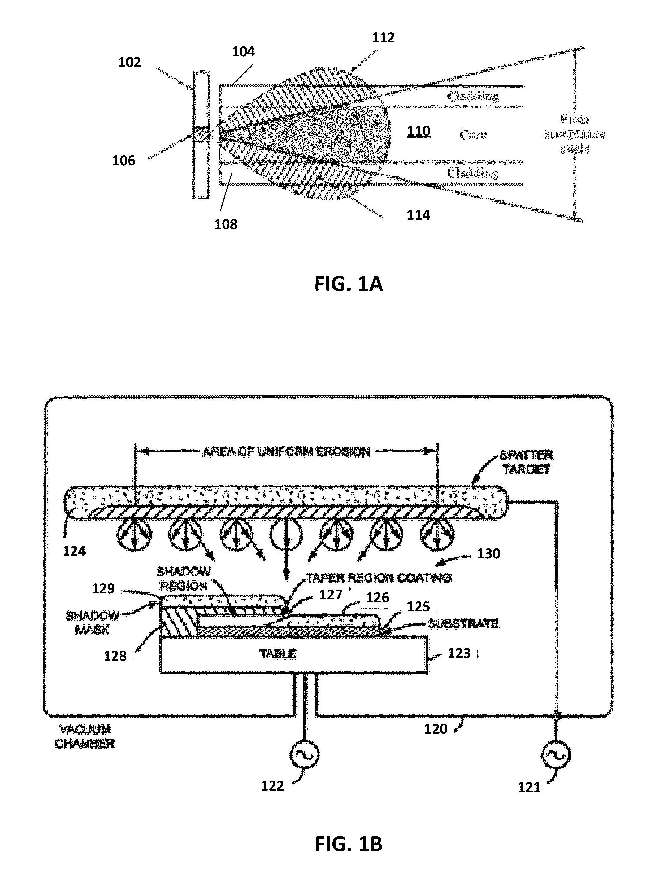
Methods of depositing materials to provide for efficient coupling of light from a first device to a second device are disclosed. In general, these methods include mounting one or more wafers on a rotating table that is continuously rotated under one or more source targets. A process gas can be provided and one or more of the source targets powered while the wafers are biased to deposit optical dielectric films on the one or more wafers. In some embodiments, a shadow mask can be laterally translated across the one or more wafers during deposition. In some embodiments, deposited films can have lateral and / or horizontal variation in index of refraction and / or lateral variation in thickness.

Description

RELATED APPLICATIONS[0001]The present application claims priority to U.S. Provisional Patent Application 61 / 725,400, filed on Nov. 12, 2012, which is herein incorporated by reference in its entirety.BACKGROUND[0002]1. Field of Invention[0003]Embodiments of the present invention are directed towards efficient coupling of light and, in particular, to adiabatic planar waveguide couplers and their applications.[0004]2. Discussion of Related Art[0005]Efficient coupling of light emitted or received by high index and high numerical aperture (NA) devices, such as organic light emitting diodes (OLEDs), light emitting diodes (LEDs) and Laser diodes, has not been available other than through discrete devices such as lenses and gratings. Such coupling is also hindered due to the lack of transparent, high index optical materials having an index n above the range of approximately 1.44 to 1.7 for such discrete devices. Transparent oxides and dielectrics are often prepared by melting or sintering o...

Claims


Application Information

Patent Timeline
Patent Type & Authority Patents(United States)
IPC IPC(8): G02B6/00G02B6/14G02B6/30G02B6/132
CPCG02B6/132G02B6/305G02B6/14C23C14/044C23C14/542C23C14/548Y10T74/18576C23C14/083G02B6/0003G02B6/122G02B6/1228G02B6/4212G02B19/0042G02B2006/12147H05K999/99
Inventor DEMARAY, R. ERNEST
Owner DEMARAY
Learn More