Eureka AIR delivers breakthrough ideas for toughest innovation challenges, trusted by R&D personnel around the world.

Imaging device, image processing device, image processing method and program

a technology of incident light and imaging device, applied in the direction of color signal processing circuit, radiation controlled device, television system, etc., to achieve the effect of easy detection of abnormal oblique incident ligh

Active Publication Date: 2016-06-07
FUJIFILM CORP
View PDF28 Cites 4 Cited by
  • Summary
  • Abstract
  • Description
  • Claims
  • Application Information

AI Technical Summary

Benefits of technology

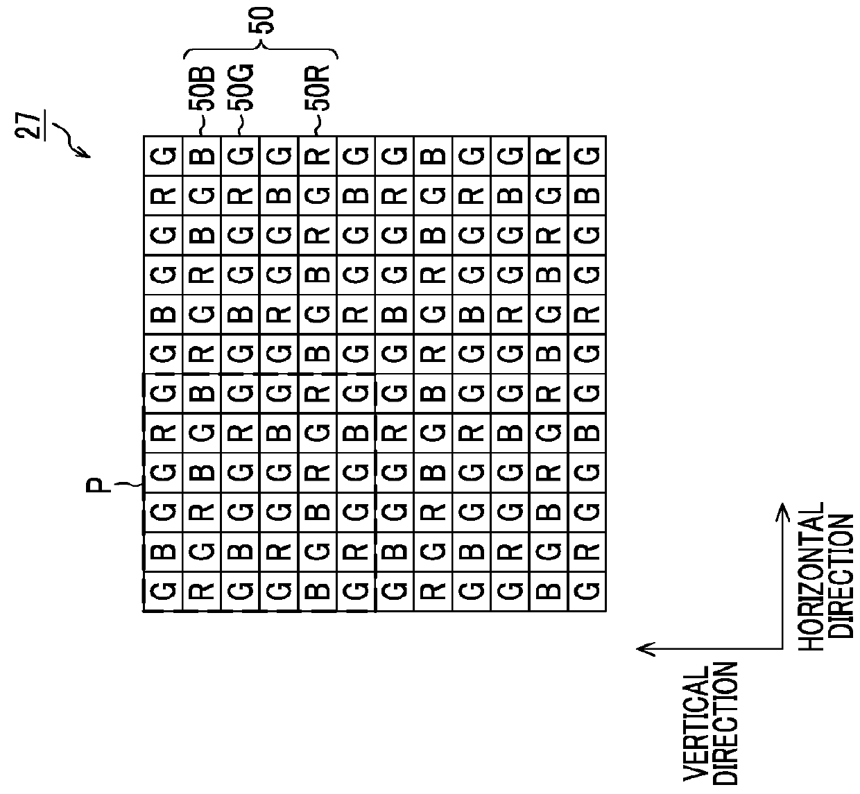
[0012]In such an imaging element having a simple color filter array, the color mixture phenomenon is also comparatively simple. Hence, it is possible to reduce the effect of color mixture on image data through comparatively easy color mixture correction.
[0066]According to the aspects of the present invention, on the basis of the average values of the respective pixel data pieces corresponding to the types of the determination pixels in the area of the imaging element, it is possible to easily detect abnormal oblique incident light which is incident into the imaging element.

Problems solved by technology

However, recently, imaging elements having comparatively complex color filter arrays are also used, and there may be multiple pixels for which types of pixels (color filters) adjacent thereto are different, even among pixels having color filters with the same color.

Method used


Image

  • Imaging device, image processing device, image processing method and program
  • Imaging device, image processing device, image processing method and program
  • Imaging device, image processing device, image processing method and program

Examples


Embodiment Construction

[0097]Referring to drawings, embodiments of the present invention will be described.

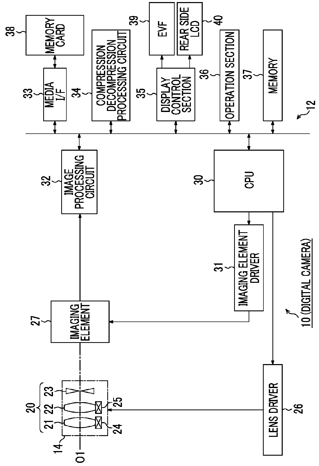
[0098]FIG. 1 is a block diagram illustrating one configuration example of a digital camera 10.

[0099]In the present example, in the configuration shown in FIG. 1, a description will be given of an example in which the respective sections other than a lens unit 14 and a lens driver 26 are provided in a camera main body 12. However, as necessary, the respective sections may be provided in the lens unit 14.

[0100]The digital camera (imaging device) 10 includes a camera main body 12, and a lens unit 14 which is mounted onto the front side of the camera main body 12 so as to be replaceable.

[0101]The lens unit 14 includes a photography optical system 20, and the photography optical system 20 includes a zoom lens 21, a focus lens 22, a mechanical shutter 23, and the like.

[0102]The zoom lens 21 and the focus lens 22 are respectively driven by a zoom mechanism 24 and a focus mechanism 25 so as to be movable alo...


PUM


Abstract

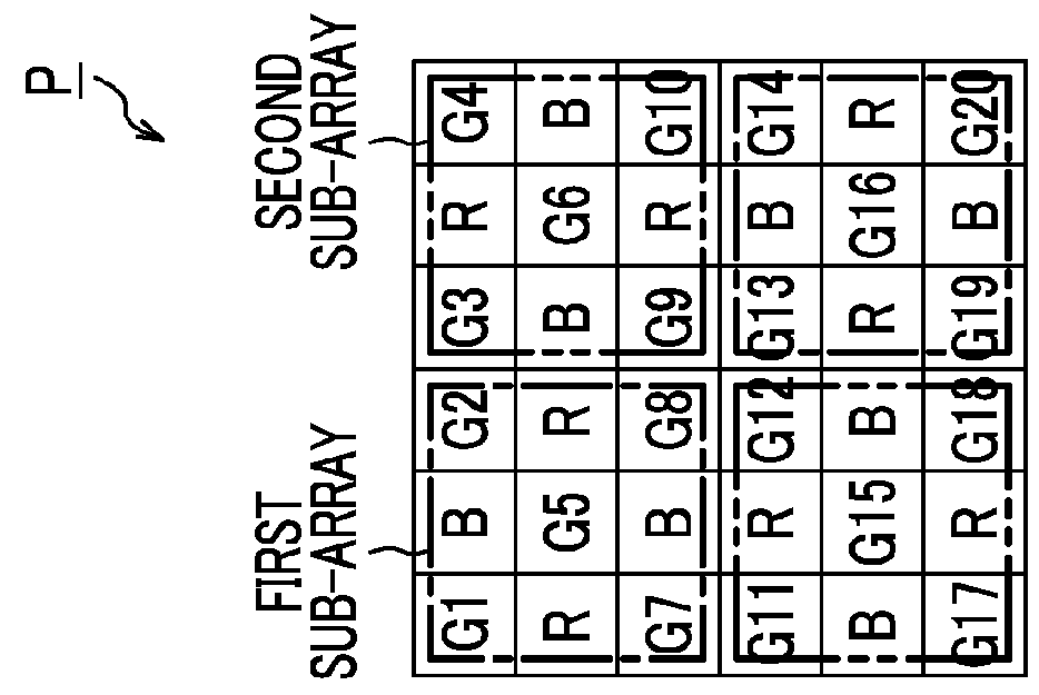
Pixels constituting the imaging element include at least four types of the determination pixels for which color filter patterns of adjacent pixels thereof are different from one another. At least one of pixels, which are adjacent to each determination pixel, is a first color pixel that has a color filter with a first color. Further, among the pixels which are adjacent to each determination pixel, a pixel, which is opposed to the first color pixel with the determination pixel interposed therebetween, has a color filter other than the color filter with the first color. Abnormal oblique incident light, which is incident into the imaging element, is detected on the basis of average values of the respective pixel data pieces corresponding to the types of these determination pixels.

Description

CROSS-REFERENCE TO RELATED APPLICATIONS[0001]This application is a Continuation of PCT International Application No. PCT / JP2014 / 53817, filed on Feb. 18, 2014, which claims priority under 35 U.S.C. §119(a) to Japanese Patent Application No. 2013-043005, filed on Mar. 5, 2013. Each of the above application(s) is hereby expressly incorporated by reference, in its entirety, into the present application.BACKGROUND OF THE INVENTION[0002]1. Field of the Invention[0003]The present invention relates to an imaging device, an image processing device, an image processing method, and a non-transitory computer readable medium. In particular, the present invention relates to a technique of detecting abnormal oblique incident light.[0004]2. Description of the Related Art[0005]Generally, in single-plate-type imaging elements having mosaic color filter arrays, color mixture is caused by light leakage from adjacent pixels. When an image is generated by performing digital signal processing on color sig...

Claims


Application Information

Patent Timeline
Patent Type & Authority Patents(United States)
IPC IPC(8): H04N9/04H04N9/73H04N9/64H04N5/374H04N5/372H04N5/359H01L27/146
CPCH04N9/045H04N5/359H04N5/372H04N5/374H04N9/646H04N9/735H01L27/14621H04N23/81H04N23/843H04N25/133H04N23/88H04N25/134H04N25/62H04N25/71H04N25/76
Inventor KAWAI, TOMOYUKIHAYASHI, KENKICHIKURAHASHI, HIDEKAZU
Owner FUJIFILM CORP
Why Eureka
Eureka Blog
Learn More