
Display device and fabrication method of display device

a display device and fabrication method technology, applied in non-linear optics, instruments, optics, etc., can solve the problems of loss of an overall reflectivity of the electrophoretic display device, adverse effect on the display quality of the display device, etc., and achieve the effect of thinning thickness and favorable display quality

Active Publication Date: 2016-04-19
E INK HLDG INC
View PDF19 Cites 1 Cited by
  • Summary
  • Abstract
  • Description
  • Claims
  • Application Information

AI Technical Summary

Benefits of technology

This patent describes a display device with good quality and a thin thickness. The invention also provides a method for making the device with a high success rate. The color filter layer is placed between the display layer and a substrate to improve the display quality, especially the viewing angle. The transparent sealing material used in this method does not require high temperatures for curing, reducing the likelihood of displacement during the fabrication process. Overall, the display device has better quality and yield.

Problems solved by technology

However, the color filter thin film, by adhering above the display medium through an optical glue or a double-sided adhesive, may increase a thickness of the electrophoretic display device, and the use of the optical glue or the double-sided adhesive may further produce a gap between an electrophoretic display layer and the thin film, thereby causing a loss in an overall reflectivity of the electrophoretic display device.
As such, in a curing process of the sealing, a relative displacement is produced between the externally adhered color filter thin film and the display layer, thereby causing an adverse effect on a display quality of the display device.

Method used


Image

  • Display device and fabrication method of display device
  • Display device and fabrication method of display device
  • Display device and fabrication method of display device

Examples


Embodiment Construction

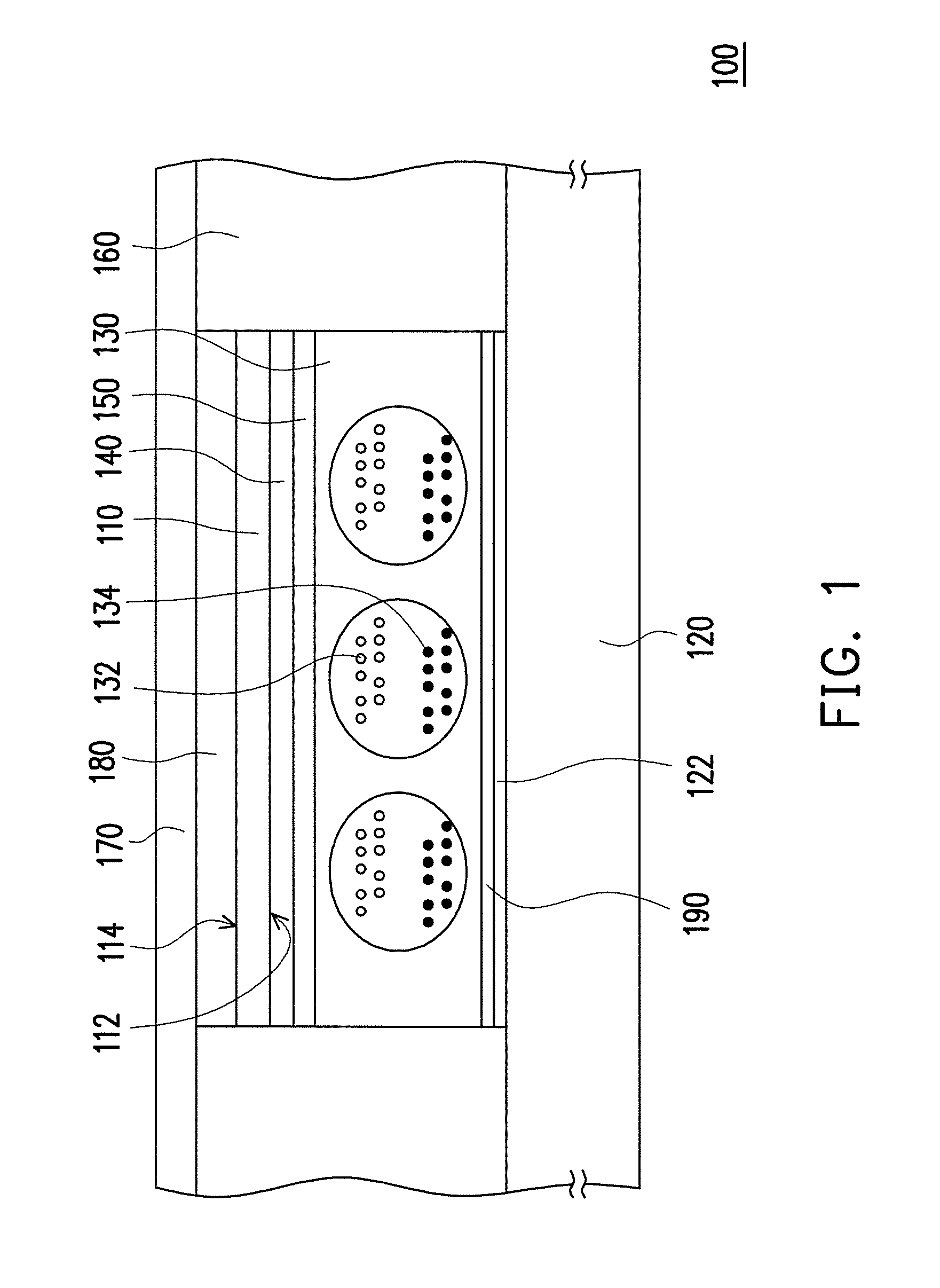
[0036]FIG. 1 is schematic diagram illustrating a display device according to an embodiment of the invention. Referring to FIG. 1, a display device 100 includes a first substrate 110, a second substrate 120, a display layer 130, a color filter layer 140, a transparent electrode layer 150, a transparent sealing 160, a protective film 170 and adhesive layers 180 and 190. The first substrate 110 is disposed opposite to the second substrate 102, and the display layer 130 is disposed between the first substrate 110 and the second substrate 120. The color filter layer 140 and the transparent electrode layer 150 are both disposed between the first substrate 110 and the display layer 130. The protective film 170 is adhered on the first substrate 110 via the adhesive layer 180 and the second substrate 120 is adhered on the display layer 130 via the adhesive layer 190. The transparent sealing 160 surrounds the display layer 130 to seal the display layer 130 between the first substrate 110 and ...


PUM

PropertyMeasurementUnit
curable temperatureaaaaaaaaaa
temperatureaaaaaaaaaa
transparentaaaaaaaaaa

Abstract

A display device including a first substrate, a second substrate, a display layer, a color filter layer, a transparent electrode layer and a transparent sealing is provided. The first substrate is opposite to the second substrate. The display layer is disposed between the first substrate and the second substrate. The color filter layer is disposed between the display layer and the first substrate. The transparent electrode layer is disposed between the color filter layer and the display layer. The transparent sealing surrounds the display layer so that the display layer is sealed between the first substrate and the second substrate, wherein a curable temperature of the transparent sealing is lower than or equal to 40° C. A fabrication method of a display device is further provided herein.

Description

CROSS-REFERENCE TO RELATED APPLICATION[0001]This application claims the priority benefit of Taiwan application serial no. 101151059, filed on Dec. 28, 2012. The entirety of the above-mentioned patent application is hereby incorporated by reference herein and made a part of this specification.BACKGROUND[0002]1. Field of the Application[0003]The invention relates to a display device, and more particularly, to a multi-color display device.[0004]2. Description of Related Art[0005]In recent year, e-paper and e-book adopt an electrophoretic display technology to achieve the purpose of display. Taken the black and white e-book for example, a display media thereof is constituted by a black electrophoretic liquid and white charged particles dispersed in the black electrophoretic liquid, and through applying voltages, the white charged particles may be driven to move, so that each pixel respectively displays a black color, white color or grayscale.[0006]In the conventional technology, most of...

Claims


Application Information

Patent Timeline
Patent Type & Authority Patents(United States)
IPC IPC(8): G02F1/167G02F1/1339G02F1/1677G02F1/1679
CPCG02F1/167G02F1/1339G02F2001/1672G02F1/1681G02F1/1679G02F1/1677
Inventor LO, PO-YUANLEE, TAI-YUAN
Owner E INK HLDG INC
Learn More