Electronics apparatus and production method for an electronics apparatus

a production method and electronic technology, applied in the direction of cross-talk/noise/interference reduction, casing/cabinet/drawer details, electric apparatus, etc., can solve the problems of unproblematically transmitting use signals via ribbon cables, attenuating electromagnetic modes that could otherwise travel into the surrounding environment in an uncontrolled manner, etc., to reduce the installation space of electronics apparatus, reduce the installation space, and easy to filter out

Active Publication Date: 2016-04-12
ROBERT BOSCH GMBH
View PDF12 Cites 0 Cited by
  • Summary
  • Abstract
  • Description
  • Claims
  • Application Information

AI Technical Summary

Benefits of technology

[0005]In accordance with the present invention, an example interference suppression design of an electronics apparatus is provided using a plurality of filters situated on at least two circuit boards, whose configuration can also be designated an “in-series connection” of the filters situated on the circuit boards. Using the interference suppression design, high-frequency, high-energy interferences can easily be filtered out. In contrast to the conventional use of expensive filters in the low-voltage area / high-voltage area, which as a rule are very expensive and require a large amount of installation space, the interference suppression design according to the present invention can be realized using filters that are inexpensive and that require little installation space. The example electronics apparatus according to the present invention and the corresponding production method thus may offer in particular a reduction of the installation space of the electronics apparatus, with low manufacturing costs and / or better interference suppression.
[0006]The present invention may be advantageous for an electronics apparatus having a high-voltage area in which high-energy high-frequency interferences can occur that conventionally can couple inside the housing and can produce electromagnetic cavity modes in connection above all with the connected cooperating devices, e.g., an engine, an electric machine, a battery, and / or a generator. In contrast, the high-frequency interferences produced in the inverting device (inverter, double inverter) of the electronics apparatus according to the present invention are transferred to other assemblies / circuit boards / hybrids inside the electronics apparatus, and interference in sensitive components / assemblies is suppressed using low-cost filters. Thus, the present invention may offer a low-cost filtering, requiring little installation space, of the connecting lines between the circuit boards and the housing potential, and thus offers a walling off of the connecting paths / coupling paths that lead from the device, in particular from the sealed and shielded high-voltage area, to the surrounding environment.
[0007]Compared to a shielding of a circuit board by a lead lining, which, due to a through-hole required for the electrical contacting of the circuit board, does not enable shielding of the circuit board against electromagnetic interferences, the “in-series connection” of the low-cost filters can also protect an electric component situated on a circuit board against electromagnetic interferences. This is ensured in particular if multi-stage filters that are low in cost and that require little installation space, each having a interference discharge line to the housing potential, are used on the connecting plugs on the circuit boards.

Problems solved by technology

In contrast, useful signals are unproblematically transmitted via a ribbon cable.
In addition, the described filters and the at least one plate-type shielding unit also bring about an attenuation of electromagnetic modes that could otherwise travel into the surrounding environment in an uncontrolled manner via a low-voltage connection.

Method used


Image

  • Electronics apparatus and production method for an electronics apparatus
  • Electronics apparatus and production method for an electronics apparatus
  • Electronics apparatus and production method for an electronics apparatus

Examples


Embodiment Construction

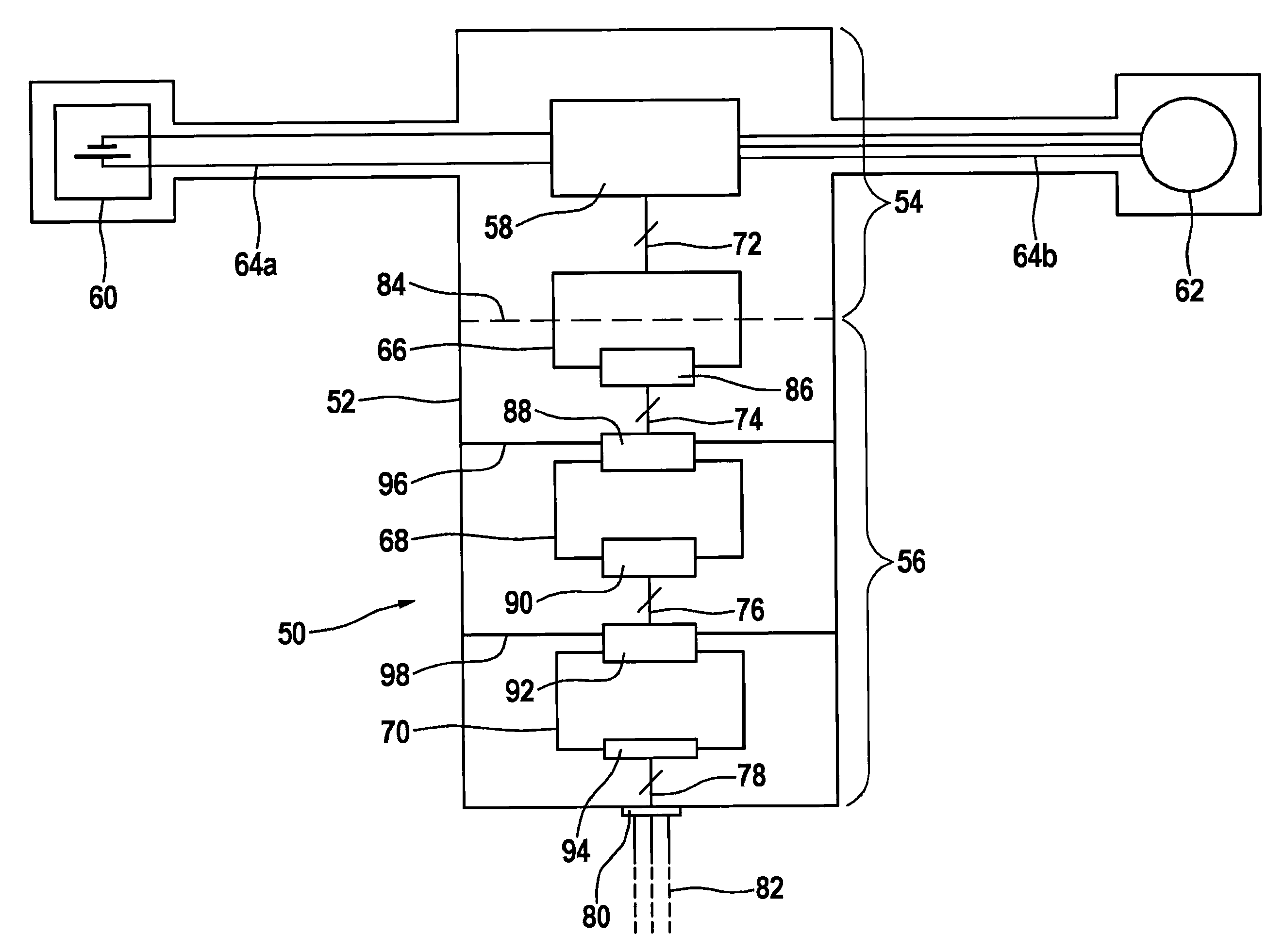
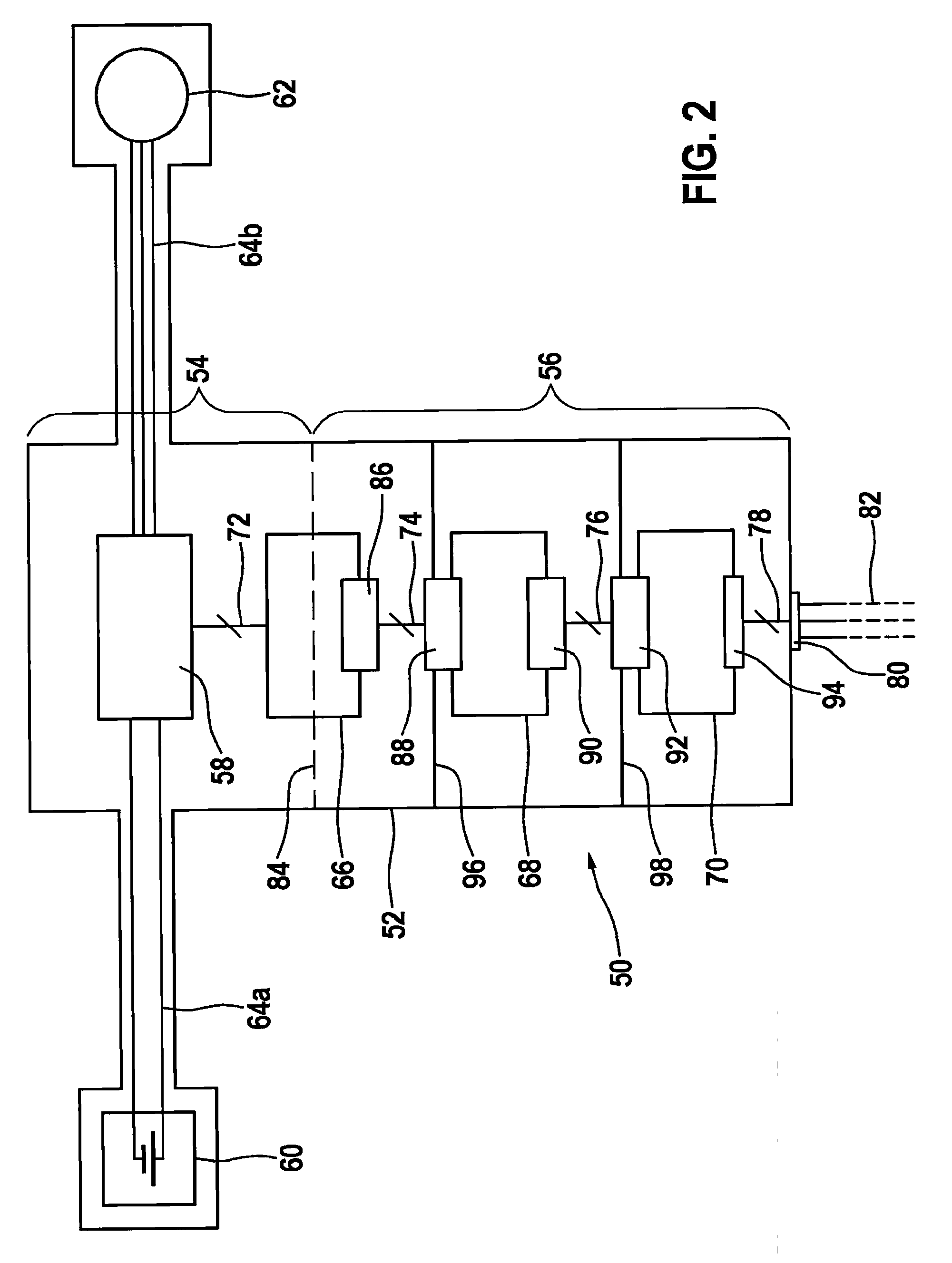
[0026]FIG. 2 shows a schematic representation of a specific embodiment of the electronics apparatus.

[0027]Electronics apparatus 50 shown schematically in FIG. 2 has an (expanded) housing 52 that is fashioned at least partly from a conductive material. The conductive material of housing 52 can be a metal and / or a doped semiconductor material. Preferably, housing 52 is made completely of the conductive material.

[0028]In the depicted specific embodiment, the interior space of housing 52 can be divided (schematically) at least into an interference area, fashioned as high-voltage area 54, and at least one area that is fashioned as low-voltage area 56 and is decoupled by the filtering described below. However, electronics apparatus 50 is not limited to such a division into at least one interference area and at least one decoupled area, or to the realization of these as high-voltage area 54 and low-voltage area 56. Instead, the depicted division is intended to demonstrate merely as an exam...


PUM

PropertyMeasurementUnit
widthaaaaaaaaaa
widthaaaaaaaaaa
widthaaaaaaaaaa

Abstract

An electronics apparatus having a housing, an inverting device, a first circuit board connected to the inverting device via at least one line, and a second circuit board connected via a first galvanic connection to the first circuit board and connected via a second galvanic connection to at least component, and having a first filter situated on the first circuit board and upstream from the first galvanic connection, the first filter having a first discharge connection to the housing, and having a second filter situated on the second circuit board and downstream from the first galvanic connection, the second filter having a second discharge connection to the housing, and having a third filter situated on the second circuit board and upstream from the second galvanic connection, the third filter having a third discharge connection to the housing. A method for producing an electronics apparatus is also described.

Description

FIELD OF THE INVENTION[0001]The present invention relates to an electronics apparatus. In addition, the present invention relates to a method for producing an electronics apparatus.BACKGROUND INFORMATION[0002]FIG. 1 shows a schematic representation of a conventional electronics apparatus. An example of such an electronics apparatus is for example the energy converter described in U.S. Published Patent Application No. 2007 / 0296271 A1.[0003]The schematically shown electronics apparatus 10 has an (expanded) housing 12 that is capable of being divided (schematically) at least into a high-voltage area 12a and a low-voltage area 12b. In high-voltage area 12a there is situated at least one inverting device 14 that is electrically connected at the input side to a battery 60 via a first electrical connection 15a, and is electrically connected at the output side to a motor 18 via a second electrical connection 15b. Low-voltage area 12b has at least one component 20 for operating electronics d...

Claims


Application Information

Patent Timeline
Patent Type & Authority Patents(United States)
IPC IPC(8): H05K5/02H02M1/44H05K1/02H05K1/14
CPCH02M1/44H05K1/0233H05K1/0262H05K1/142Y10T29/4913
Inventor SPARKA, HARTMUT
Owner ROBERT BOSCH GMBH
Why Eureka
Try Eureka