Adapter and electrical connection system

a technology of electrical connection and adapter, which is applied in the direction of electrical apparatus, connection, coupling device connection, etc., can solve the problems of large insertion force, interruption of electrical conduction, and unaddressed need in the art, and achieve the effect of reducing the width of the slo

Active Publication Date: 2015-12-29
LOTES
View PDF3 Cites 4 Cited by
  • Summary
  • Abstract
  • Description
  • Claims
  • Application Information

AI Technical Summary

Benefits of technology

[0031]Compared with the related art, certain embodiments of the present invention, among other things, have the following beneficial advantages.
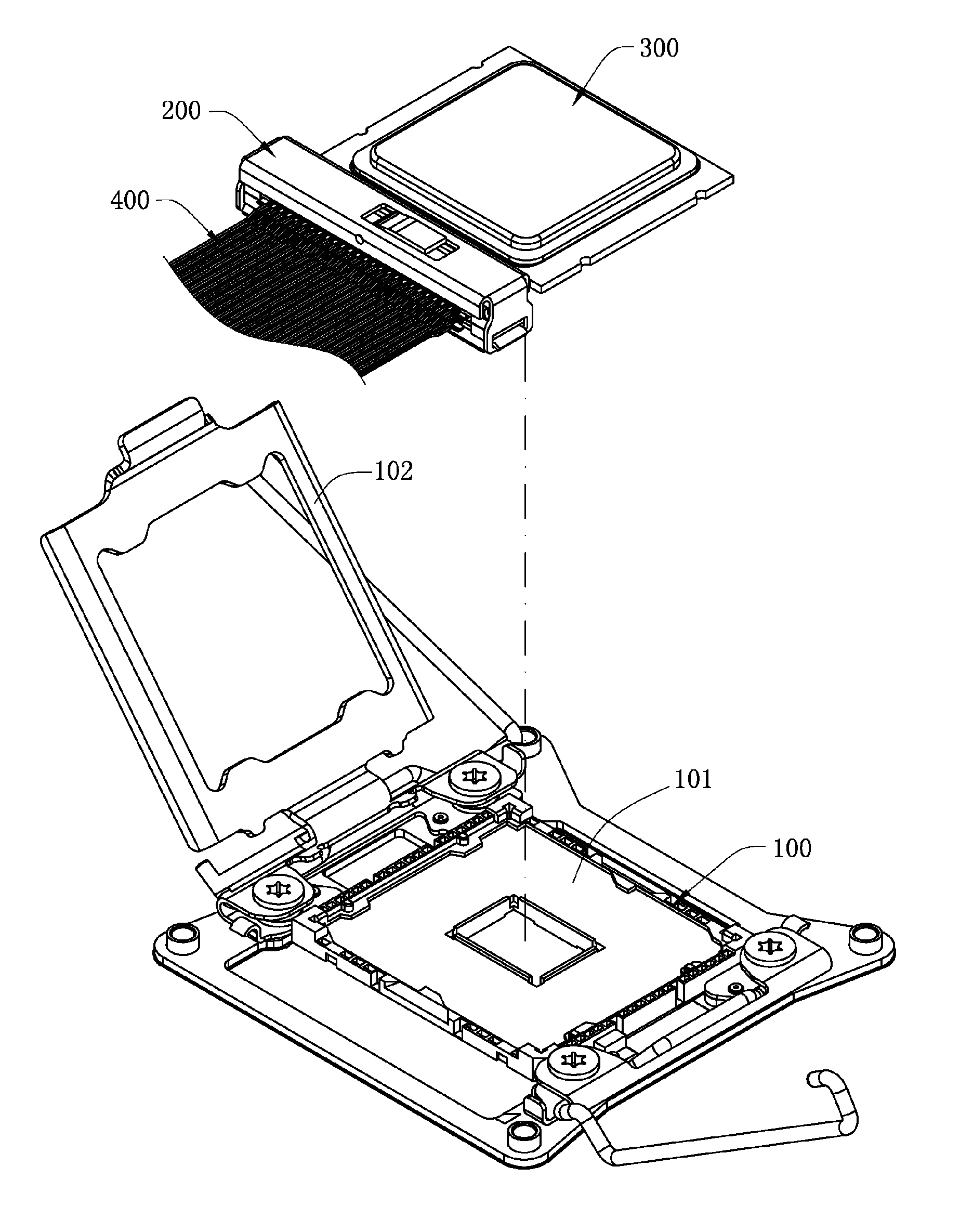
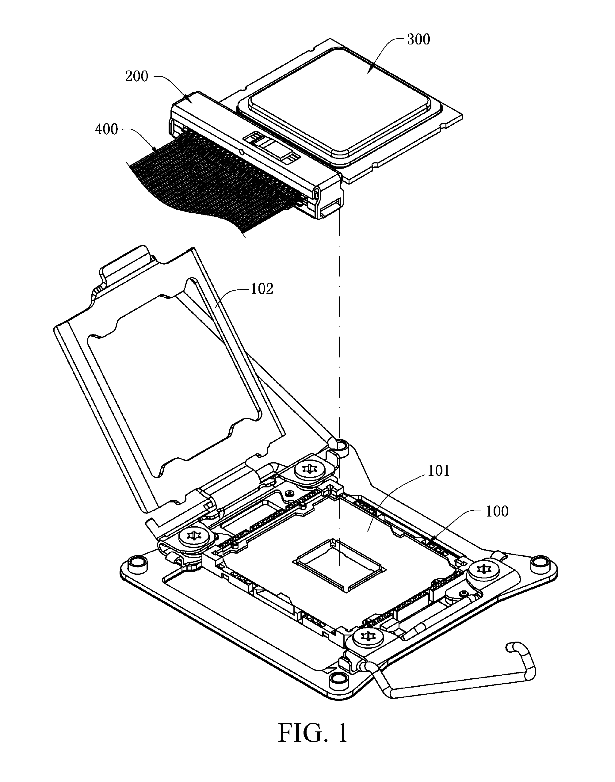
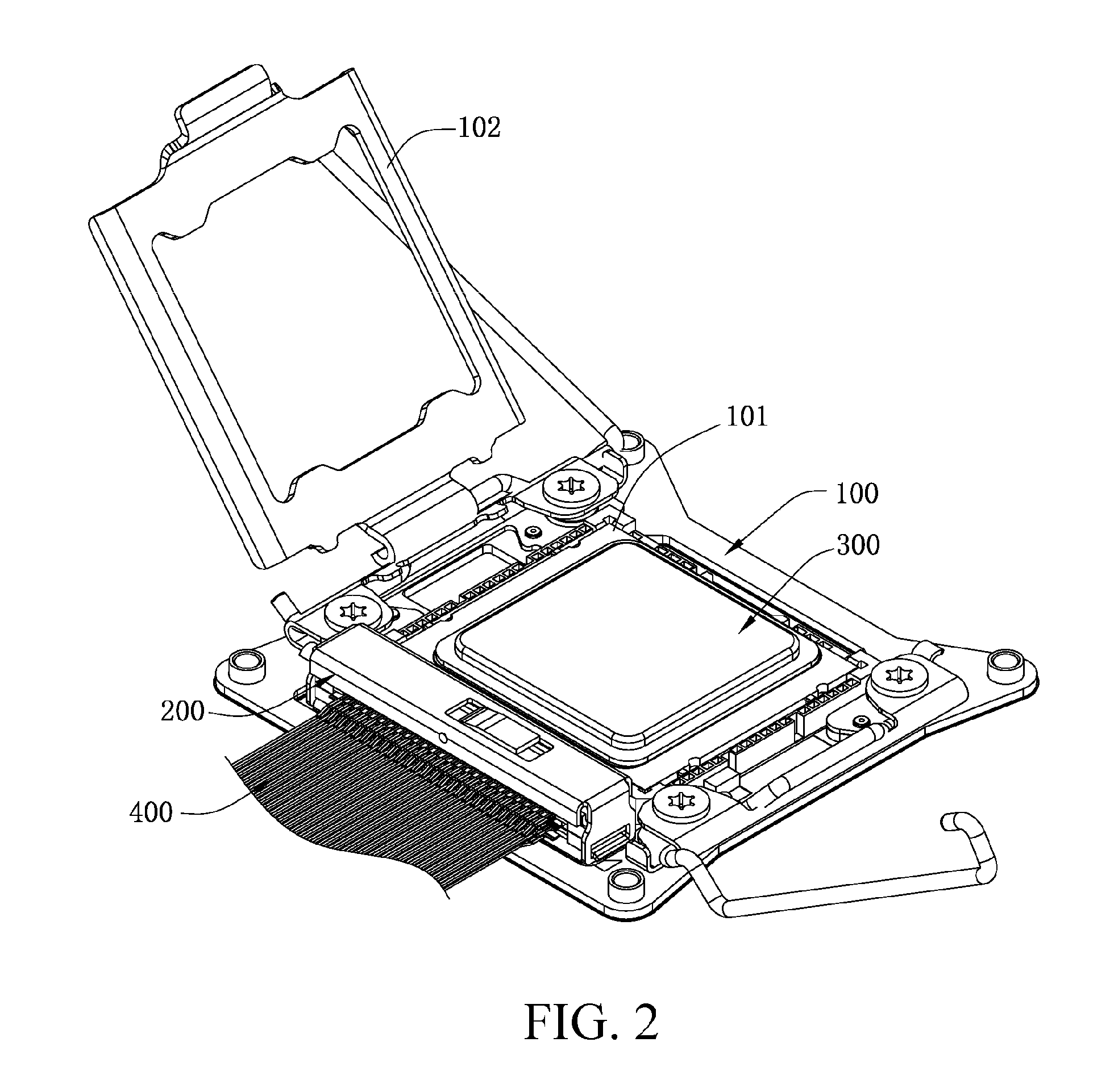
[0032]The slot is formed between the two rows of terminals in the adapter and provided for insertion of the conducting portion. When the chip module is not inserted in the slot, the width of the slot is greater than the thickness of the conducting portion, so that a zero insertion force is required for insertion of the chip module, and the conducting portion may not be worn out. After the chip module is inserted in the slot, under the effect of an external force, the width of the slot is reduced so that the terminals urge against the conducting portion, which ensures close electrical connection between the terminals and the chip module.

Problems solved by technology

However, when the distance between the two rows of the contact portions is smaller than the thickness of the first insertion portion, a large insertion force is required for insertion of the first chip module in the edge connector.
Therefore, when the first insertion portion is inserted in the first insertion port, a large insertion force is needed, and the terminals may wear out the first insertion portion, causing interruption of the electrical conduction.
Therefore, a heretofore unaddressed need exists in the art to address the aforementioned deficiencies and inadequacies.

Method used


Image

  • Adapter and electrical connection system
  • Adapter and electrical connection system
  • Adapter and electrical connection system

Examples


Embodiment Construction

[0047]The present invention is more particularly described in the following examples that are intended as illustrative only since numerous modifications and variations therein will be apparent to those skilled in the art. Various embodiments of the invention are now described in detail. Referring to the drawings, like numbers indicate like components throughout the views. As used in the description herein and throughout the claims that follow, the meaning of “a”, “an”, and “the” includes plural reference unless the context clearly dictates otherwise. Also, as used in the description herein and throughout the claims that follow, the meaning of “in” includes “in” and “on” unless the context clearly dictates otherwise. Moreover, titles or subtitles may be used in the specification for the convenience of a reader, which shall have no influence on the scope of the present invention.

[0048]It will be understood that when an element is referred to as being “on” another element, it can be di...


PUM


Abstract

An electrical connection system includes an electrical connector electrically connected to a chip module, and an adapter disposed on one side of the electrical connector. The chip module laterally extends to form a conducting portion. Two rows of terminals are disposed in the adapter, and form a slot therebetween for the conducting portion to be inserted therein. When the conducting portion is not inserted in the slot, the width of the slot is greater than the thickness of the conducting portion, so that a zero insertion force is required for insertion of the chip module. After the chip module is inserted in the slot, under the effect of an external force, the width of the slot is reduced to an extent that the terminals urge against the conducting portion, which ensures close electrical connection between the terminals and the chip module.

Description

CROSS-REFERENCE TO RELATED APPLICATION[0001]This non-provisional application claims priority and the benefit of U.S. Provisional Application No. 61 / 813,263, filed Apr. 18, 2013, the entire contents of which are hereby incorporated by reference.[0002]Some references, if any, which may include patents, patent applications and various publications, may be cited and discussed in the description of this invention. The citation and / or discussion of such references, if any, is provided merely to clarify the description of the present invention and is not an admission that any such reference is “prior art” to the invention described herein. All references listed, cited and / or discussed in this specification are incorporated herein by reference in their entireties and to the same extent as if each reference was individually incorporated by reference.FIELD OF THE INVENTION[0003]The present invention relates generally to an adapter and an electrical connection system, and more particularly to ...

Claims


Application Information

Patent Timeline
Patent Type & Authority Patents(United States)
IPC IPC(8): H01R12/88H01R12/79H01R12/72H01R12/77H01R13/193
CPCH01R12/88H01R12/79H01R13/193H01R12/774H01R12/721
Inventor JU, TED
Owner LOTES
Why Eureka
Try Eureka