Semiconductor light emitting element

a technology of semiconductor light emitting element and semiconductor, which is applied in the direction of semiconductor devices, basic electric elements, electrical appliances, etc., can solve the problems of film thickness fluctuation and difficulty in uniform formation of films, and achieve the effects of reducing production costs, preventing complexity during production, and simplifying production steps

Active Publication Date: 2015-11-17
FUJIFILM CORP
View PDF14 Cites 0 Cited by
  • Summary
  • Abstract
  • Description
  • Claims
  • Application Information

AI Technical Summary

Benefits of technology

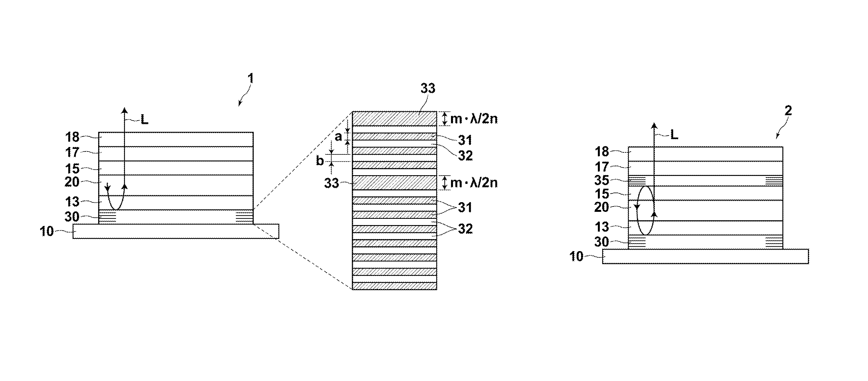
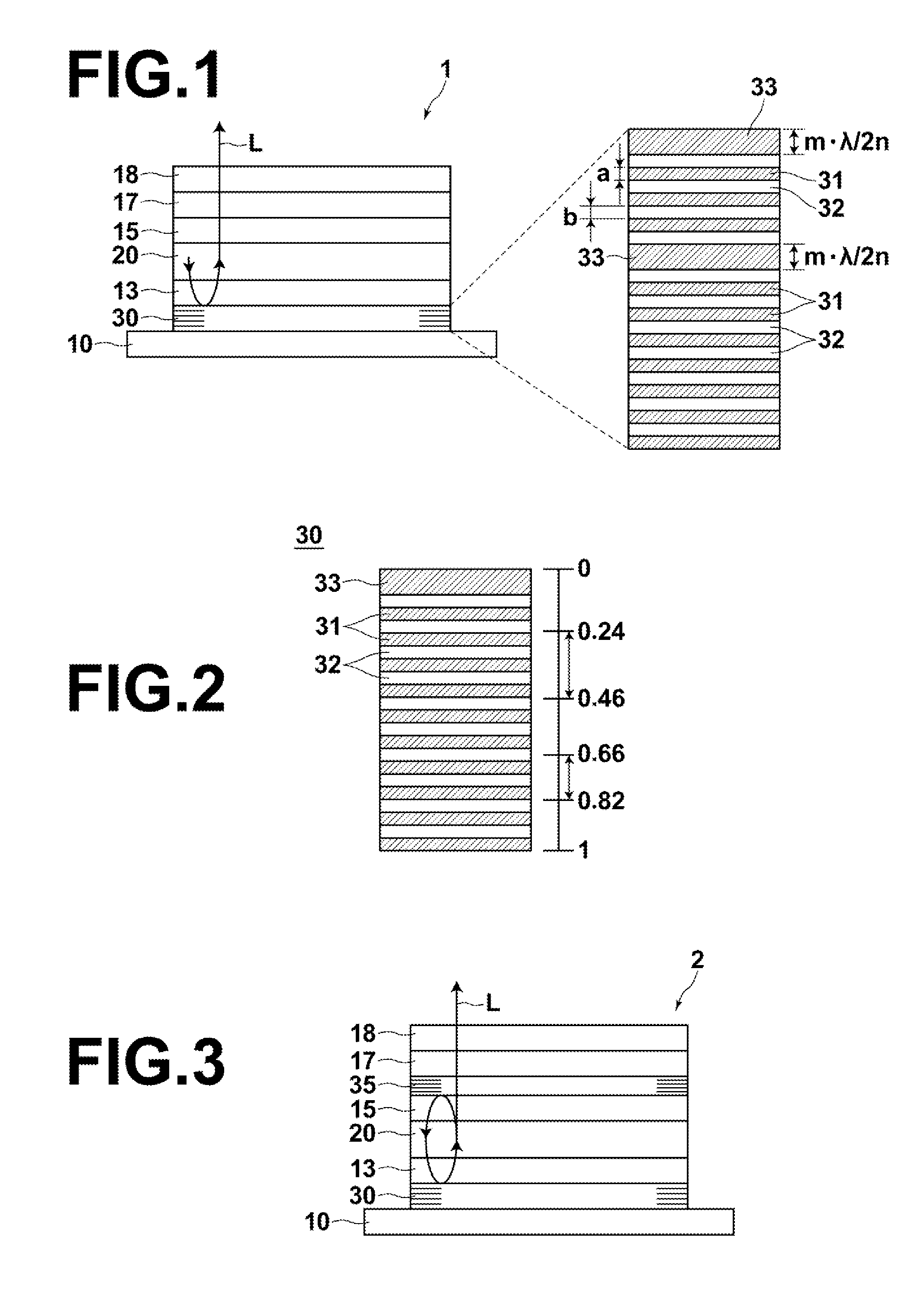
[0066]FIG. 3 is a schematic sectional view that illustrates a semiconductor light emitting element 2 according to an example of a design modification. Here, an upper DBR layer 35 is provided above a light emitting layer 20. The configuration of a lower DBR layer 30 is substantially the same as that described above, and the same advantageous effects of obtaining the light intensity enhancing effect while suppressing fluctuations in temperature properties can be obtained.
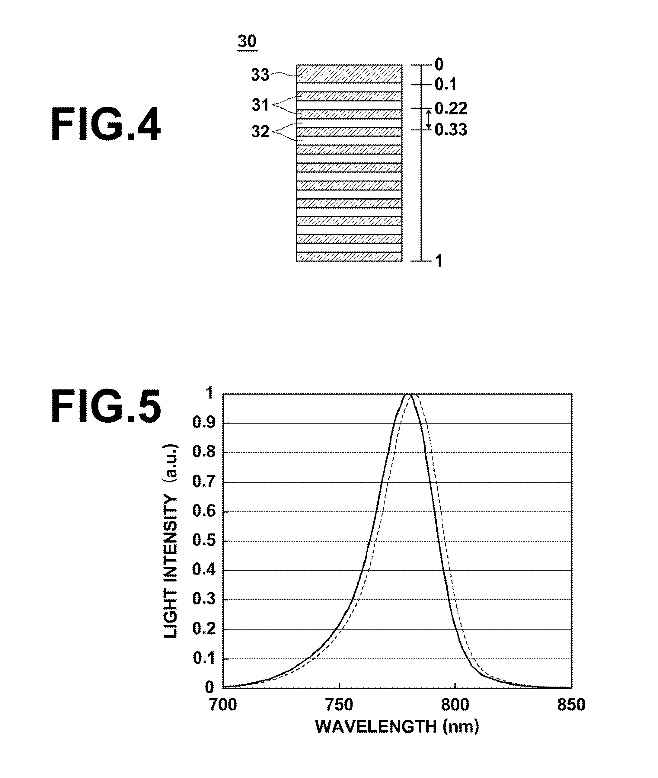
[0067]However, in the present configuration, the preferred ranges of positions at which two phase changing layers are provided in the lower DBR layer 30 differ from the embodiment described above. It is preferable for a first phase changing layer 33 to be provided within the pair closest to the light emitting layer 20, as illustrated in the schematic sectional view of the lower DBR layer 30 of FIG. 4. Meanwhile, it is preferable for a second phase changing layer 33 to be positioned within a range from 0.22 to 0.33, when the thickness of the lower DBR layer is divided into percentages, with the side thereof toward the light emitting layer designated as 0, and the side thereof toward the substrate designated as 1, as illustrated in FIG. 4 (refer to Simulation 4 to be described later).
[0068]It is preferable for the DBR layer and the light emitting layer to be of the same compositional type, in order to prevent complexities during production. The phase changing layers may be of a composition completely different from the basic layers that constitute the DBR layer. However, it is preferable for the composition of the high refractive index layers or the composition of the low refractive index layers that constitute the basic DBR layer to be employed as the composition of the phase changing layer, from the viewpoint of simplification of production steps. Note that in the embodiment described above, the thicknesses of the low refractive index layers were changed, but the same advantageous effects can be obtained by changing the thicknesses of the high refractive index layers.
[0069]In addition, in the case that a plurality of the phase changing layers are provided, film formation conditions must be calculated for each composition and film thickness in order to form the phase changing layers of different compositions and / or film thicknesses in actual production. Therefore, this will lead to an increase in development costs. Accordingly, in the case that a plurality of the phase changing layers are formed, they are constituted by layers having the same composition. In addition, the optimal thickness of the phase changing layers is λ / 2n (refer to Simulation 3 to be described later), and therefore it is preferable for the thicknesses of the phase changing layers to be the same (λ / 2n).
[0070]Note that the phase changing layers having thicknesses of mλ / 2n described in the above embodiment may have an extremely thin layer having a thickness of up to approximately 15 nm inserted within the interiors thereof (refer to simulation 5 to be described later). As long as the thickness of the inserted layer is up to approximately 15 nm, the advantageous effect of suppressing fluctuations in temperature properties can be sufficiently obtained, without losing the function of the phase changing layer.
[0071]Hereinafter, Simulations, Examples, and Comparative Examples that led to the discovery of the preferred configurations of the present invention that achieve the advantageous effects of maintaining the light intensity enhancing effect of the DBR while suppressing temperature induced changes in light intensity (temperature properties) caused by changes in ambient temperature and fluctuations in film thicknesses during production will be described.<Simulation Method>

Problems solved by technology

In actuality, however, it is difficult to form films uniformly, and fluctuations are generated in the film thicknesses.

Method used


Image

  • Semiconductor light emitting element
  • Semiconductor light emitting element
  • Semiconductor light emitting element

Examples


example 1

[0114]Example 1 is an LED having the layer structure of Simulation 2 illustrated in FIG. 11, in which the thicknesses t of the No. 1 and No. 7 low refractive index layers are λ / 2n. The resonator spectrum of this element obtained by simulations is illustrated in FIG. 17. In addition, the natural light emitting spectrum, the reflectance of the lower DBR layer with respect to the peak light emission wavelength, and the reflectance of the upper AR layer with respect to the peak light emission wavelength are illustrated in FIG. 18.

example 2

[0115]Example 2 is an LED having the layer structure illustrated in FIG. 19. In the present element, the thicknesses of the high refractive index layers 32 under the No. 1 and No. 7 low refractive index layers within the lower DBR layer are changed to λ / 2n (=116 nm) to become phase changing layers. The resonator spectrum of the present element obtained by simulations is illustrated in FIG. 20.

example 3

[0116]Example 3 is an LED having the layer structure of Simulation 5 illustrated in FIG. 15, in which the thickness of the layer 34 inserted into the No. 7 low refractive index layer is 10 nm.


PUM


Abstract

A semiconductor light emitting element that outputs emitted light having a predetermined emitted light peak wavelength λ includes: at least a substrate; a lower distributed Bragg reflector layer provided on the substrate; and a light emitting layer provided on the lower distributed Bragg reflector layer. At least one phase changing layer having a thickness of mλ / 2n (wherein n is the refractive index of the phase changing layer, and m is an integer 1 or greater) is provided within the lower distributed Bragg reflector layer.

Description

CROSS REFERENCE TO RELATED APPLICATIONS[0001]The present application is a Continuation of PCT International Application No. PCT / JP2013 / 000933 filed on Feb. 20, 2013, which claims priority under 35 U.S.C. §119(a) to Japanese Patent Application No. 2012-035076 filed on Feb. 21, 2012. Each of the above applications is hereby expressly incorporated by reference in its entirety, into the present application.BACKGROUND OF THE INVENTION[0002]1. Technical Field[0003]The present invention is related to a surface emitting type semiconductor light emitting element equipped with a distributed Bragg reflector and an active layer which are sequentially grown on a semiconductor substrate.[0004]2. Background Art[0005]There are semiconductor light emitting elements, such as light emitting diodes (LED's) and semiconductor lasers (LD's: Laser Diodes) which are configured with DBR's (Distributed Bragg Reflectors) in order to improve the light emitting efficiency thereof (Japanese Unexamined Patent Publ...

Claims


Application Information

Patent Timeline
Patent Type & Authority Patents(United States)
IPC IPC(8): H01L33/46H01L33/60H01L33/10H01L33/30
CPCH01L33/46H01L33/10H01L33/60H01L33/30
Inventor HAKUTA, SHINYA
Owner FUJIFILM CORP
Why Eureka
Try Eureka