
Reducing bowing bias in etching an oxide layer

a technology of oxide layer and etching, which is applied in the field of electronic devices manufacturing, can solve the problems of increasing the bowing profile of the sidewall, reducing the diameter of the trench and even the etch stop, and conventional techniques failing to recognize or address the bowing increase, etc., and achieves the effect of increasing the sidewall passivation and reducing the bowing profil

Active Publication Date: 2015-10-20
TOKYO ELECTRON LTD
View PDF16 Cites 0 Cited by
  • Summary
  • Abstract
  • Description
  • Claims
  • Application Information

AI Technical Summary

Benefits of technology

[0008]The invention decreases the bowing profile without adversely affecting the trench diameter or causing etch stop. For example, bowing in an oxide layer of a multi-layer stacked trench capacitor can be reduced by process changes (of gas chemistry) in poly-Si or SOI layers underneath it. For example, techniques can include altering gas chemistry (Nitrogen and Argon) that is contributing to the ion-etching of poly-Si (or SOI) layer without altering diameters of other layers in the trench. Flow rates of nitrogen and argon and the ratio of nitrogen to argon can also be controlled. The invention also includes selectively altering gas chemistry to increase sidewall passivation at a specific location without closing off a trench.

Problems solved by technology

Because of the increased lateral etch during the poly-Si etch, the conventional sidewall passivation becomes insufficient to protect the trench from bowing.
Unfortunately, increasing the flow of the polymerizing gas can also lead to a decrease in trench diameter and even etch stop.
Conventional techniques also fail to recognize or address increases in bowing that can occur in etching multiple layers between the oxide layer and the silicon substrate.
Some conventional techniques include increasing mask thickness above the oxide layer, but this is undesirable because many processes / design parameters specify decreased thicknesses of amorphous carbon and SiARC layers above the oxide.

Method used


Image

  • Reducing bowing bias in etching an oxide layer
  • Reducing bowing bias in etching an oxide layer
  • Reducing bowing bias in etching an oxide layer

Examples


Embodiment Construction

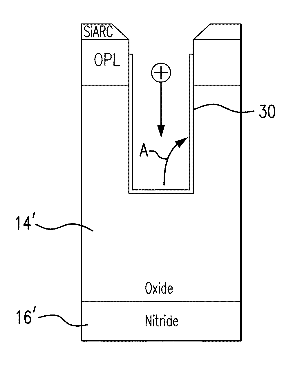
[0014]Techniques disclosed herein include systems and methods for reducing bowing bias in an oxide layer during etching of multi-layered deep trenches using targeted over passivation of sidewalls. In plasma etching, the substrate is placed on a substrate holder of a process chamber, and gases (forming the process chemistry) are supplied to the process chamber. In addition, power (e.g. RF power) is applied to one or more electrodes to form a plasma.

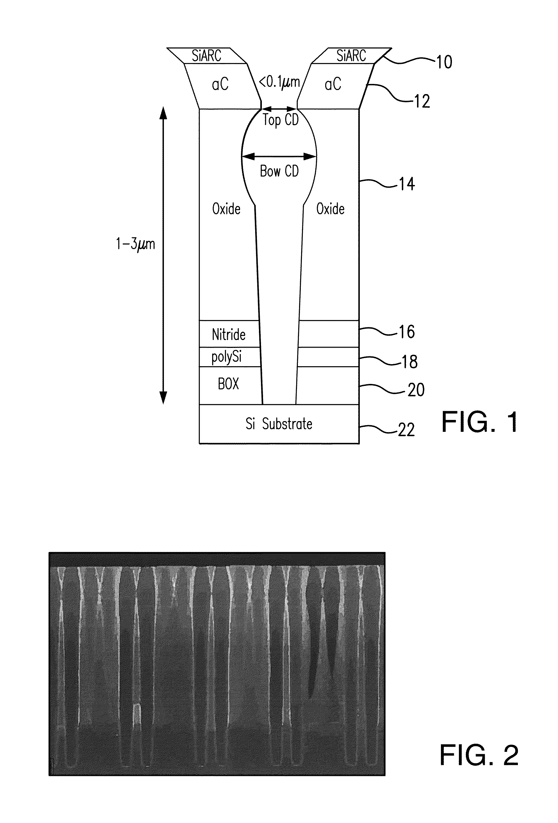
[0015]A deep trench mask open process involves etching through various layers of a given substrate stack. The stack can include layers such as: SiARC (Silicon anti-reflective coating), amorphous carbon (aC), oxide, nitride, polysilicon, buried oxide, and a silicon substrate. Oxide etch is mainly an ion-assisted process. Ions are bombarded onto a reactive surface of the oxide layer leading to an anisotropic etch. To protect sidewalls from etching, fluorocarbon based gases are used for passivation.

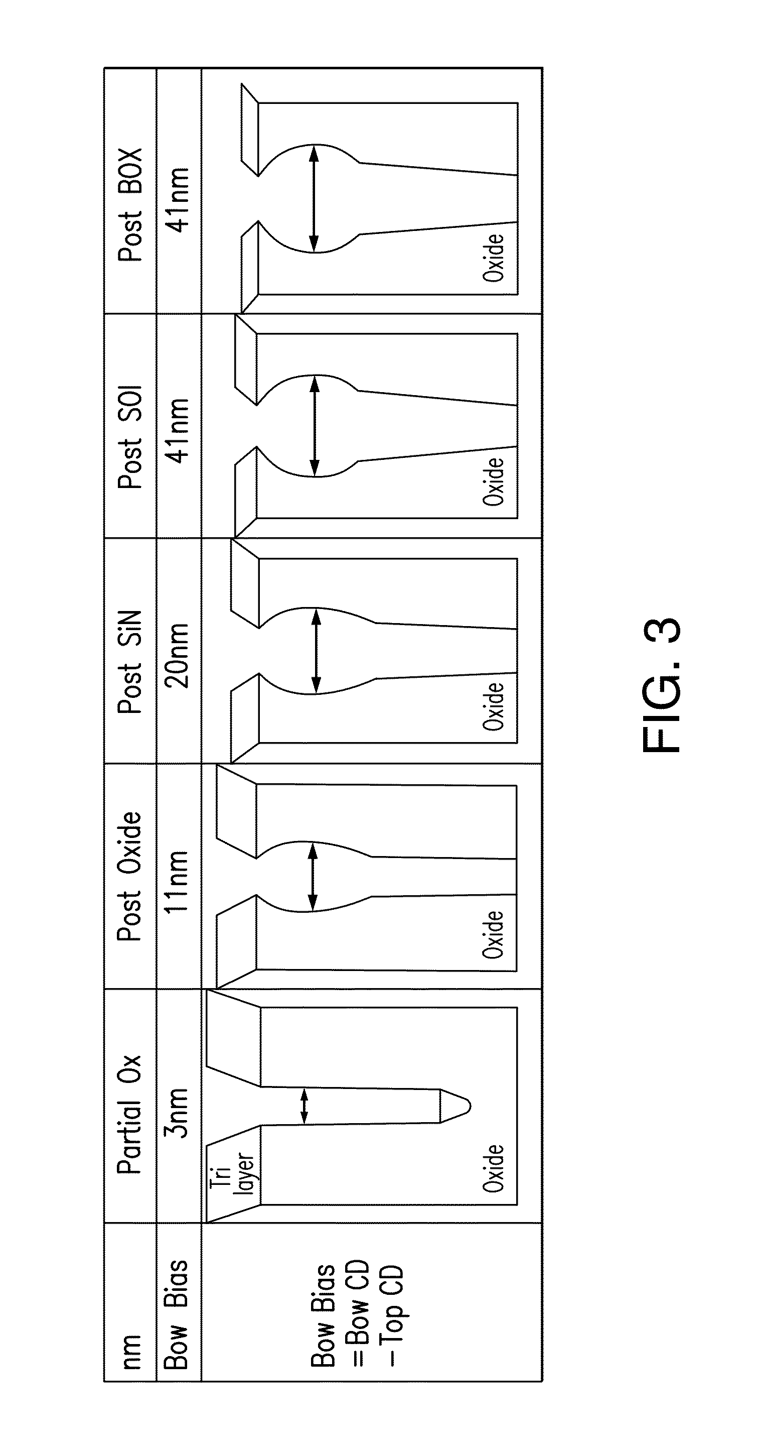
[0016]Bowing primarily occurs in an upper pa...


PUM


Abstract

An etching method in which bowing or lateral etching is reduced or minimized, particularly with respect to bowing which can occur in etching of an oxide layer in high aspect ratio structures. It has been recognized that such bowing typically occurs in the upper portion of the oxide layer in terms of its location, but that the timing at which the bowing occurs is during the etching of the lower regions of the oxide layer and also during etching of a poly-Si or SOI layer located under the oxide layer. In a preferred form, a thicker passivation layer is formed in the upper region of the oxide layer and a thinner passivation layer is formed when etching the lower portion of the oxide layer or deeper in the etch trench. As a result, reduction in the passivation layer in the upper region which can occur during etching of the lower or deeper region of the trench can be accommodated by the increased thickness passivation layer. In addition, the bowing can be additionally reduced by accelerating the poly-Si or SOI etch, for example, by poly-Si simultaneously using both argon and nitrogen during the etch.

Description

CROSS REFERENCE TO RELATED APPLICATIONS[0001]This application claims priority to provisional application 61 / 806,561 filed Mar. 29, 2013, the entirety of which is incorporated herein by reference.FIELD OF THE INVENTION[0002]The invention relates to fabrication of electronic devices such as semiconductors, and particularly to a method for reducing bowing in etching to form such devices. The invention can be particularly advantageous in manufacturing memory devices.BACKGROUND OF THE INVENTION[0003]Fabrication of semiconductor devices involves multi-step processes of forming features on a semiconductor substrate. Steps can include material growth, patterning, doping, deposition, etching, metallization, planarization, and so forth. Techniques herein relate to etching features in semiconductor substrates. Such features can include trenches, vias, through-silicon-vias, and other patterns etched in wafers or other substrates. Etching of substrates typically involves using a plasma processin...

Claims


Application Information

Patent Timeline
Patent Type & Authority Patents(United States)
IPC IPC(8): H01L21/3065H01L21/311H01L21/3213H01L49/02
CPCH01L21/31116H01L21/31144H01L21/32137H01L28/90
Inventor AVASARALA, BHARAT K.
Owner TOKYO ELECTRON LTD
Learn More