
Infrared light detector having high resolution

a high-resolution, infrared light technology, applied in the field can solve the problem of too large area of infrared light detectors, and achieve the effects of stable structure, low response time of sensor chips, and high thermal conductivity

Active Publication Date: 2015-06-02
AVAGO TECH INT SALES PTE LTD
View PDF10 Cites 0 Cited by
  • Summary
  • Abstract
  • Description
  • Claims
  • Application Information

AI Technical Summary

Benefits of technology

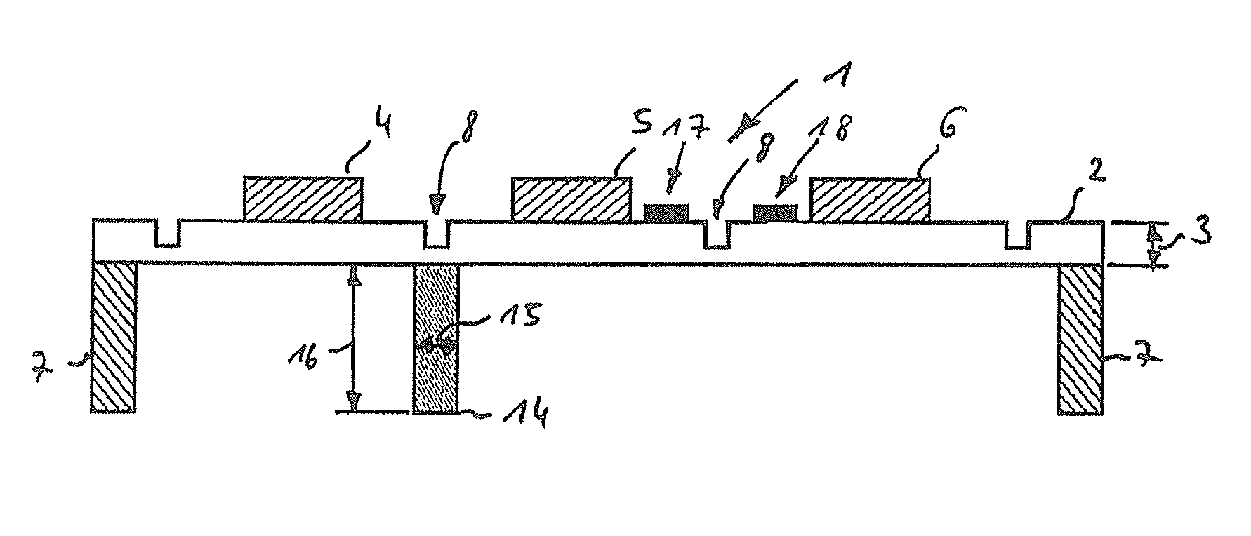
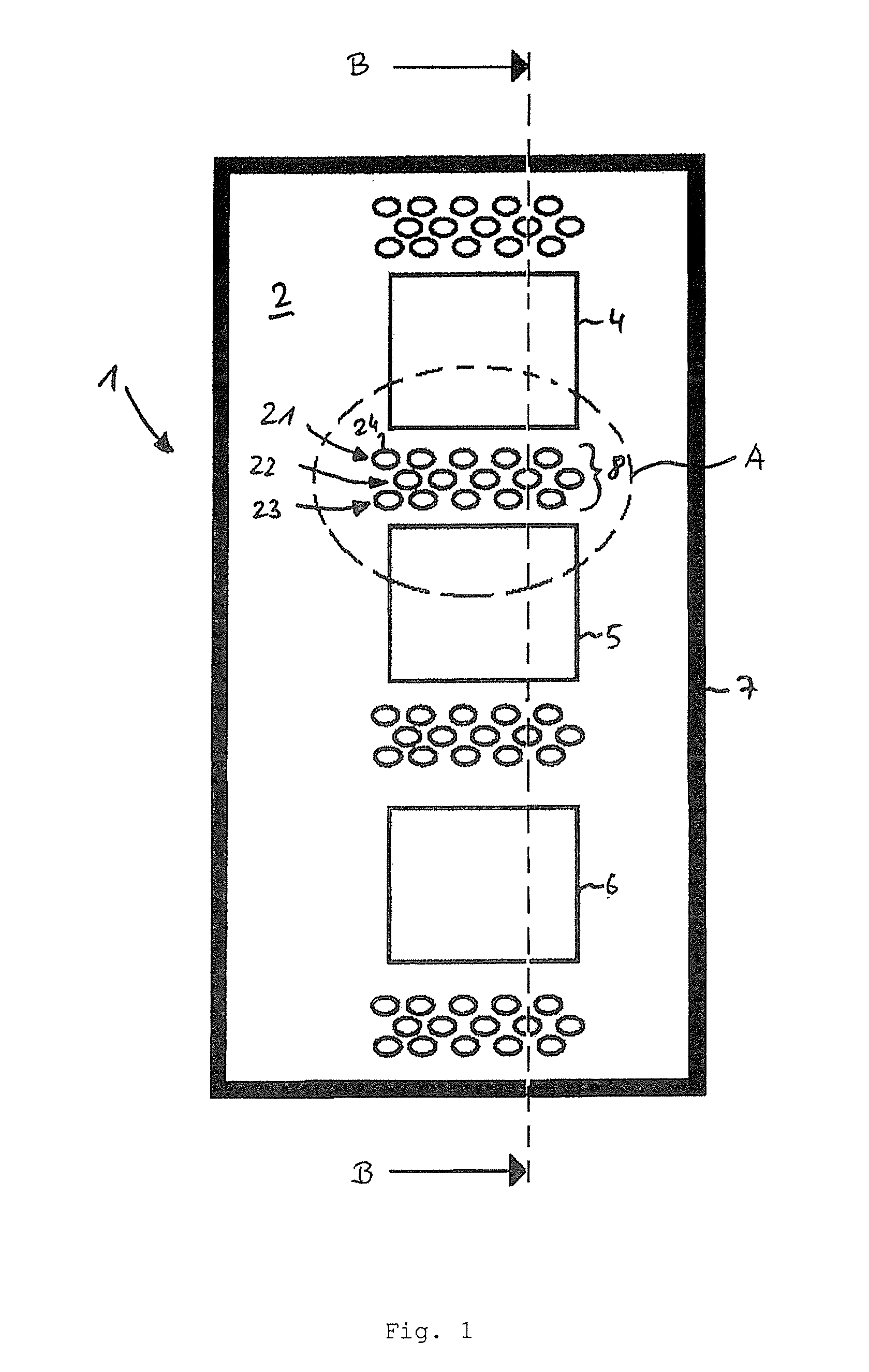
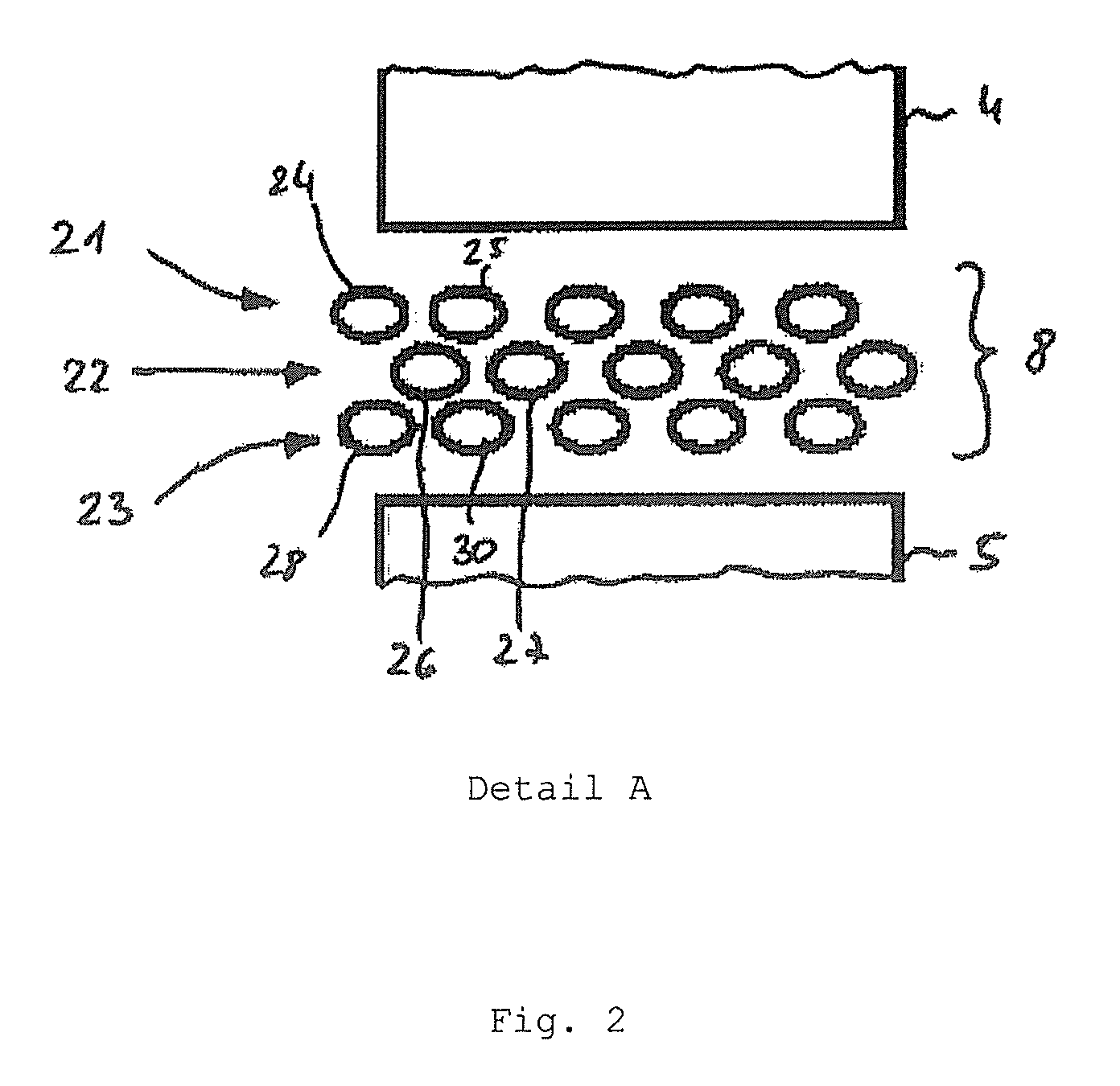
[0010]The thermal conduction from the one sensor chip to the other sensor chip takes place in the material of the carrier membrane. In that material of the carrier membrane is removed at the holes of the hole track, thermal conduction is suppressed via the holes. Only the material of the carrier membrane that resides between the holes thus remains for the heat transfer from the one sensor chip to the other sensor chip. The holes of the adjacent hole tracks are offset, so the distance from the one sensor chip to the other sensor chip through the material of the carrier membrane meanders in the region of the hole tracks and thus is designed to be longer in comparison with the straight-line connection between two sensor chips. For this reason the path of the thermal conduction from the one sensor chip to the other sensor chip is extended through the material of the carrier membrane. The heat input into the one sensor chip with lower temperature by a sensor chip with higher temperature is thereby smaller. Crosstalk of the sensor chips due to heat exchange is thus reduced. The spatial resolution of the infrared light detector is thereby high, wherein the population density of the carrier membrane with the sensor chips is high.
[0011]The region of the carrier membrane that is provided with the hole tracks thermally insulates two adjacent sensor chips since a smaller amount of heat is transferred from the one sensor chip to the other sensor chip. For this reason the sensor chips can be heated quickly by the radiant heat, and the increase of the electrical signals of the sensor chips at the point in time of the incidence of the radiant heat on the sensor chips is advantageously steep. The infrared light detector according to the invention thus has a shorter response time.
[0014]Due to the insulation effect of the hole tracks, upon ending the thermal radiation the sensor chip can only be cooled slowly by heat discharge via the carrier membrane. This would have the consequence that the decline of the electrical signal is flat at the point in time of the absence of the thermal radiation on the sensor chip. The provision of the thermal conductor strip with which heat can be quickly conducted away from the sensor chip achieves a remedy, such that due to the heat discharge by means of the thermal conductor strip the sensor chip cools rapidly upon the absence of the thermal radiation by heat discharge via the thermal conductor strip. The decline of the electrical signal is thereby steep at the point in time of the absence of the thermal radiation at the sensor chip. The response time of the infrared light detector is thus low even though the infrared light detector can have a high population density with the sensor chips.
[0016]At least one rib is preferably attached, running between the sensor chips, on the side of the carrier membrane that faces away from said sensor chips, said rib having a higher thermal conductivity than the carrier membrane and being connected in a thermally conductive manner with the senor chips via the carrier membrane so that heat can be dissipated from the sensor chips with the rib, whereby the response time of the sensor chips is low. In that the rib is arranged on the side of the carrier membrane facing away from the sensor chips, the rib can preferably be attached in the region of the carrier membrane in which the hole tracks are provided. A portion of the heat flow that passes through the region of the carrier membrane with the hole tracks is thereby dissipated by the rib, such that the heat flow that passes from one sensor chip to the other sensor chip via the region of the carrier membrane with the hole tracks is reduced.
[0018]At least one of the holes preferably has a round cross section, wherein alternatively at least one other of the holes has an oval cross section. The notch stress effect caused by the provision of the holes of the hole tracks in the carrier membrane is thereby reduced, whereby this carrier membrane has a high strength. The oval cross section preferably has its major semi-axis aligned with the course of the appertaining hole track. The strength of the material of the carrier membrane is thereby reduced between the individual holes of the appertaining hole track, whereby the heat flow through the carrier membrane is reduced transversal to the hole tracks.

Problems solved by technology

A sensor chip that, for example, is not activated due to a momentary infrared light exposure is heated by a different sensor chip located in its surroundings, which has the consequence of an unwanted activation of this sensor chip.
However, this measure has the disadvantage that the areal extent of the infrared light detector is too large due to the large distances between the sensor chips.

Method used


Image

  • Infrared light detector having high resolution
  • Infrared light detector having high resolution
  • Infrared light detector having high resolution

Examples


Embodiment Construction

[0023]As is clear from FIGS. 1 through 5, an infrared light detector 1 has a carrier membrane 2 that is designed with a membrane thickness 3. The carrier membrane 2 forms a substrate for a first sensor chip 4, a second sensor chip 5 and a third sensor chip 6. In FIG. 1, 3 through 5, the sensor chips 4 through 6 are attached equidistantly next to one another. Provided on the outer edge of said carrier membrane 2, on its underside, is a supporting frame 7 that surrounds the carrier membrane 2 and supports this.

[0024]The sensor chips 4 through 6 comprise pyroelectric material, such that upon their exposure with infrared light—in particular in a wavelength range between 3 through 20 μm—a corresponding electrical signal is present at the sensor chips 4 through 6.

[0025]Upon exposure of the sensor chips 4 through 6 with the infrared light, this is absorbed by the sensor chips 4 through 6 such that the sensor chips 4 through 6 heat up. Given a different heating of the sensor chips 4 through...


PUM


Abstract

An infrared light detector has a carrier membrane with at least two sensor chips thereon located next to each other. The carrier membrane has at least two rows of holes therein, proceeding parallel to each other between the sensor chips. The respective holes in one of the rows are offset with respect to the holes in an adjacent row, thereby hindering heat transmission via the carrier membrane between the sensor chips.

Description

BACKGROUND OF THE INVENTION[0001]1. Field of the Invention[0002]The invention concerns an infrared light detector with high resolution and high structural density.[0003]2. Description of the Prior Art[0004]It is known to use infrared light to detect gas. With a suitable light source the gas to be detected is exposed with infrared light, wherein a portion of the infrared light is absorbed by the gas such that a residual light remains. The residual light can be measured with an infrared light sensor with which the wavelength range and / or the intensity of the residual light can be detected and correspondingly transduced into an electrical signal. Given a suitable evaluation, the type and content of the detected gas can be concluded based on the electrical signal.[0005]The infrared light detector has a number of sensor chips that are arranged in a grid arrangement on a carrier membrane. The sensor chips are conventionally produced from a layer with pyroelectrically sensitive material, f...

Claims


Application Information

Patent Timeline
Patent Type & Authority Patents(United States)
IPC IPC(8): G01J5/02G01J5/34H01L31/024H01L31/09
CPCG01J5/34G01J5/0225H01L31/024H01L31/09
Inventor FREEBORN, SCOTT
Owner AVAGO TECH INT SALES PTE LTD
Learn More