
Three-dimensional memory and method of forming the same

a three-dimensional memory and memory technology, applied in the field of three-dimensional memory and a method of forming the same, can solve the problem of bottleneck in the miniaturization of storage memory cells, and achieve the effect of improving uniformity and reliability of the devi

Active Publication Date: 2015-05-05
MACRONIX INT CO LTD
View PDF7 Cites 5 Cited by
  • Summary
  • Abstract
  • Description
  • Claims
  • Application Information

AI Technical Summary

Benefits of technology

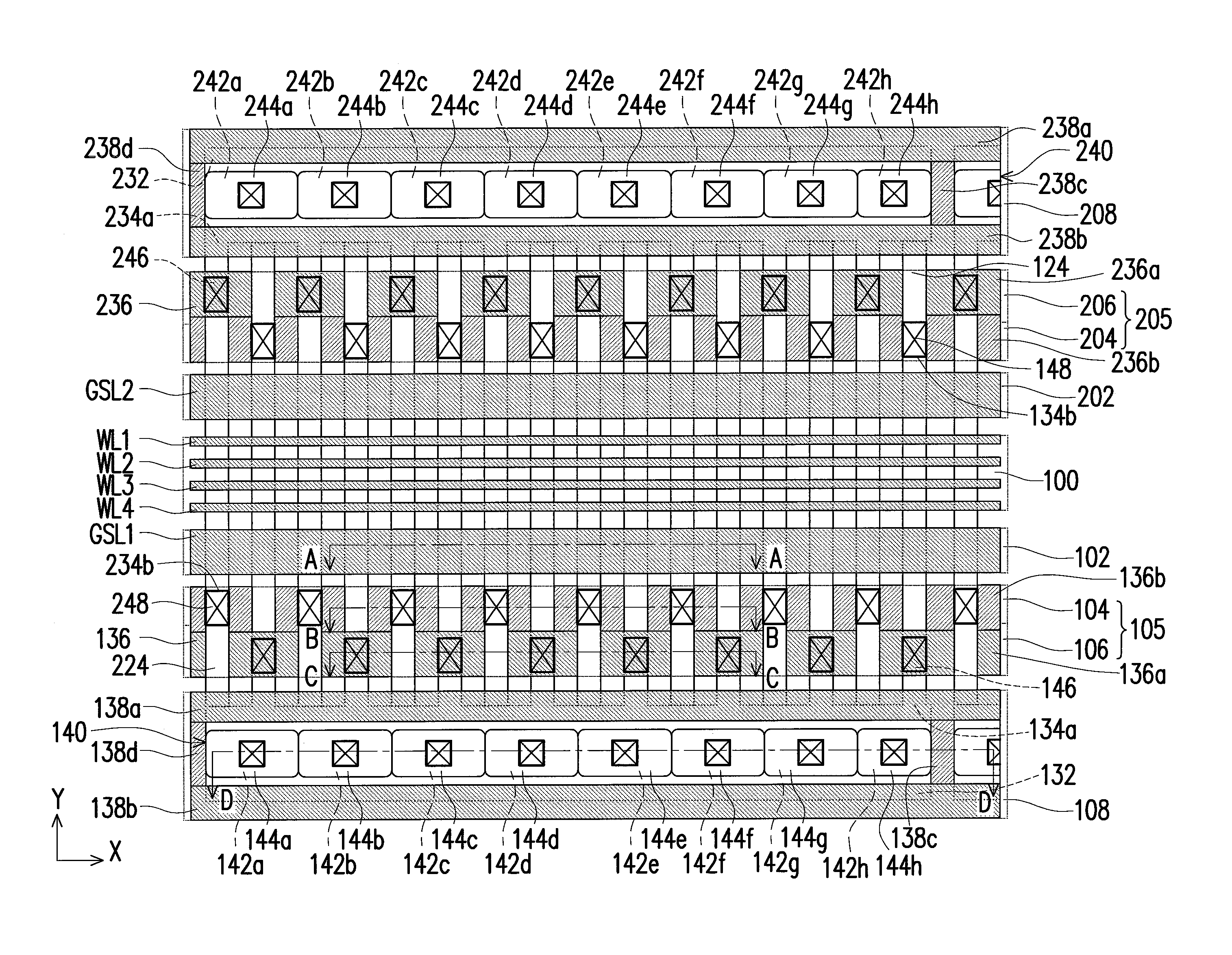
The present invention provides a three-dimensional memory and a method of forming the same with improved uniformity and reliability. In one embodiment, a low resistance path is generated to increase the turn-on current. The three-dimensional memory has a stepped structure with a doped region formed at the surface of the semiconductor layer below each step surface, which results in substantially the same junction depth and concentration. Additionally, the invention includes optional second auxiliary gates that are disposed on the charge storage layer between the ground select lines and the bit line pad. The second auxiliary gates can reduce the turn-on resistance and increase the turn-on current.

Problems solved by technology

However, the existing planar NAND flash memory is limited by the device critical dimension in integrated circuits, so that the miniaturization of storage memory cells faces a bottleneck.

Method used


Image

  • Three-dimensional memory and method of forming the same
  • Three-dimensional memory and method of forming the same
  • Three-dimensional memory and method of forming the same

Examples


Embodiment Construction

[0024]Reference will now be made in detail to the present preferred embodiments of the invention, examples of which are illustrated in the accompanying drawings. Wherever possible, the same reference numbers are used in the drawings and the description to refer to the same or like parts.

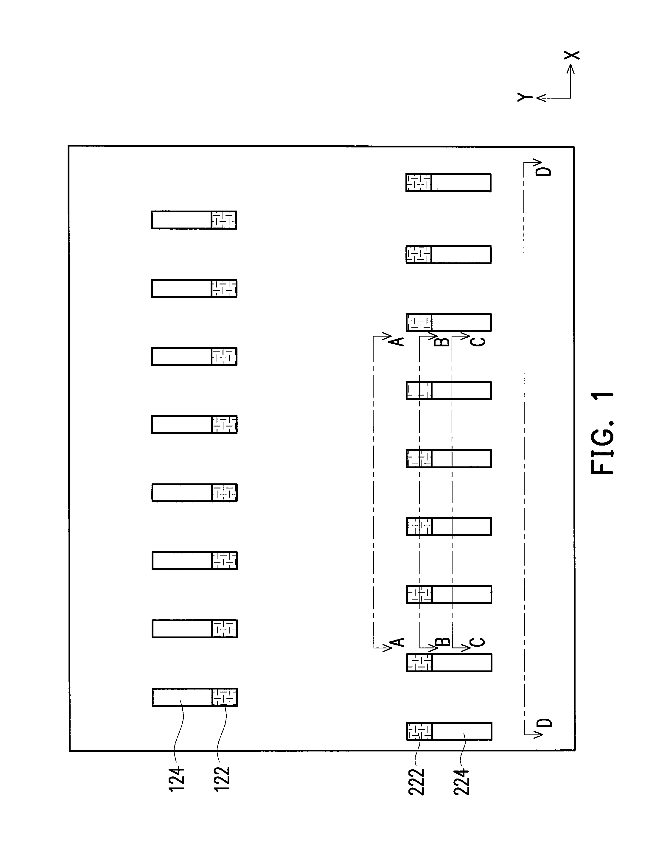
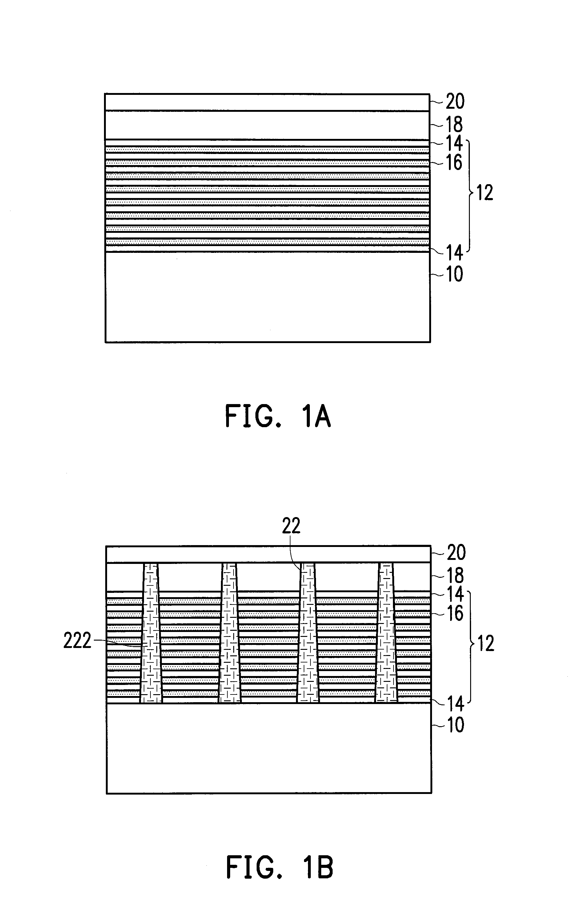
[0025]FIG. 1 to FIG. 8 are top views illustrating a method of forming a three-dimensional memory according to an embodiment of the present invention. FIG. 1A to FIG. 8A are cross-sectional views taken along the line A-A of FIG. 1 to FIG. 8. FIG. 1B to FIG. 8B are cross-sectional views taken along the line B-B of FIG. 1 to FIG. 8. FIG. 1C to FIG. 8C are cross-sectional views taken along the line C-C of FIG. 1 to FIG. 8. FIG. 1D to FIG. 8D are cross-sectional views taken along the line D-D of FIG. 1 to FIG. 8.

[0026]Referring to FIG. 1 to FIG. 1D, a stacked structure 12 is formed on a substrate 10. The stacked structure 12 includes a plurality of insulating layers 14 and a plurality of semiconductor lay...


PUM


Abstract

A method of forming a three-dimensional memory is provided. A stacked structure is patterned to form a comb structure including a bit line pad extending along a first direction and comb-teeth portions extending along a second direction. A charge storage layer is formed on top and sidewall of the comb structure. Bit lines and auxiliary gates are formed on the charge storage layer and extend along the first direction. Each bit line covers top and sidewall of partial comb-teeth portions. Auxiliary gates cover top and sidewall of edge regions of the bit line pad. The charge storage layer on top of the bit line pad is removed. The stacked structure of the bit line pad is patterned to form a stepped structure. An ion implantation is performed to the stepped structure, to form a doped region in the semiconductor layer below each step surface of the stepped structure.

Description

BACKGROUND OF THE INVENTION[0001]1. Field of Invention[0002]The present invention relates to a semiconductor device and a method of forming the same, and more particularly to a three-dimensional memory and a method of forming the same.[0003]2. Description of Related Art[0004]As the demand for storage subsystems of consumer products is increased, the standard for the reading / writing speeds or capacities of products is higher, and thus, high-capacity related products have become the mainstream in the industry. Accordingly, the development of memory, especially NAND flash memory, has to respond to this demand.[0005]However, the existing planar NAND flash memory is limited by the device critical dimension in integrated circuits, so that the miniaturization of storage memory cells faces a bottleneck. Therefore, in order to achieve a greater storage capacity and a lower cost per bit, designers seek for a three-dimensional NAND flash memory with multiple planes.SUMMARY OF THE INVENTION[000...

Claims


Application Information

Patent Timeline
IPC IPC(8): H01L21/336H01L29/788H01L21/265H01L21/768H01L27/115H01L29/423
CPCH01L27/11582H01L27/11556H01L21/265H01L29/42328H01L29/42344H01L29/42376H01L21/76897H10B43/10H10B43/50H10B43/27
Inventor LEE, GUAN-RU
Owner MACRONIX INT CO LTD
Learn More