
Anti-blooming circuit for integrating photodiode pre-amplifiers

a photodiode and pre-amplifier technology, applied in the field of circuits, can solve the problems of affecting the output voltage of the supply, affecting the performance of the supply, and being susceptible to large optical exposures, so as to minimize complexity, space, and cost, and achieve maximum performance.

Active Publication Date: 2014-12-30
BAE SYST INFORMATION & ELECTRONICS SYST INTEGRATION INC
View PDF3 Cites 0 Cited by
  • Summary
  • Abstract
  • Description
  • Claims
  • Application Information

AI Technical Summary

Benefits of technology

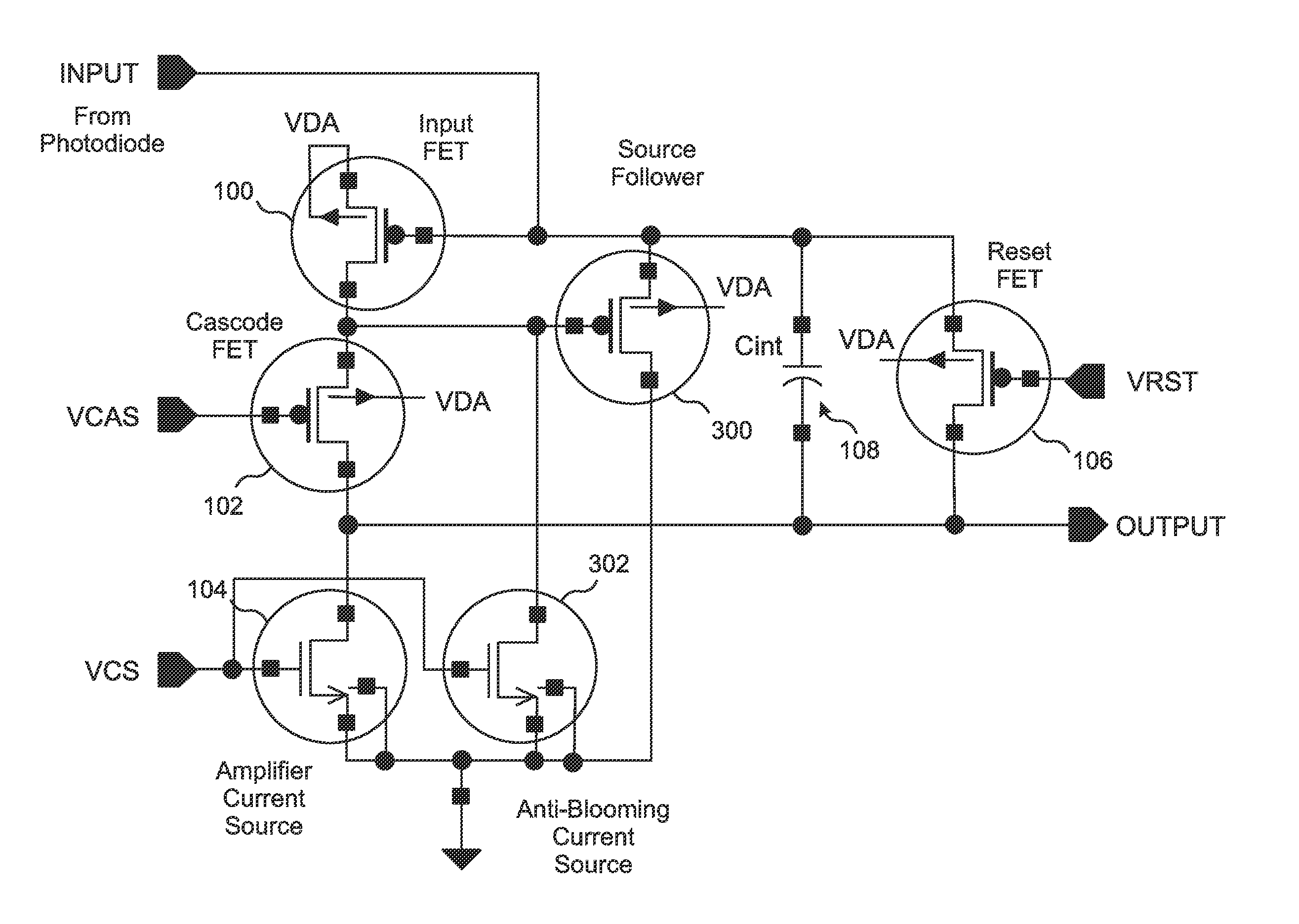
[0018]The present invention is a preamplifier input clamping circuit that maximizes performance while minimizing complexity, space, and cost. A clamping transistor, typically a clamping FET, is gated by the drain voltage of the input stage of the preamplifier, which is typically an input FET. The invention capitalizes on the fact that the initial effect of an input overload on a photo-sensor preamplifier is that its input transistor is turned off, and its drain voltage will thereby go toward ground. Accordingly, the clamping transistor is activated automatically and immediately when the input transistor begins to turn off. It is not necessary to provide or to adjust a separate anti-blooming reference voltage. The clamping behavior is sharp and substantially complete, since the clamping transistor is driven directly by the input transistor, and not by a static reference voltage.
[0019]In essence, the input transistor functions as part of the clamping circuit, so that significantly improved clamping performance is realized without adding additional circuit complexity.

Problems solved by technology

For some applications, an FPA may be susceptible to very large optical exposures that can at least temporarily blind photo-sensors and / or the optical apparatus as a whole.
When a photo-sensor is exposed to an excess of light, it is unavoidable that it will be saturated and temporarily blinded.
This effect is often referred to as “blooming.” This problem can be especially problematic when the preamplifiers are integrating preamplifiers.
Since the voltage supply for the photodiode is designed to support the normally small diode photocurrent, this sudden jump in current can exceed the voltage supply's current capacity, thereby causing the supply's output voltage to change.
Hence, if a saturated photo-sensor in the array becomes forward-biased and causes the biasing voltage supply to change, this will affect not only the saturated photo-sensor, but also all of the other photo-sensors that are supported by that same biasing supply, causing a saturated “white spot” in a resulting image to “bloom” outward from the saturated pixels to other, surrounding pixels that are not directly saturated.
As a result, a significant portion of the image can be lost.
Of course, the preamplifiers associated with any such “bloomed” pixels will also require a recovery time after the saturating light is removed, before they can once again provide undistorted output.
Unfortunately, adding circuitry to limit the photodiode output voltage rise to as small a value as possible, while not appreciably affecting preamplifier speed or noise performance, and by using as simple a circuit as possible, are inherently conflicting requirements that necessarily entail a performance compromise.
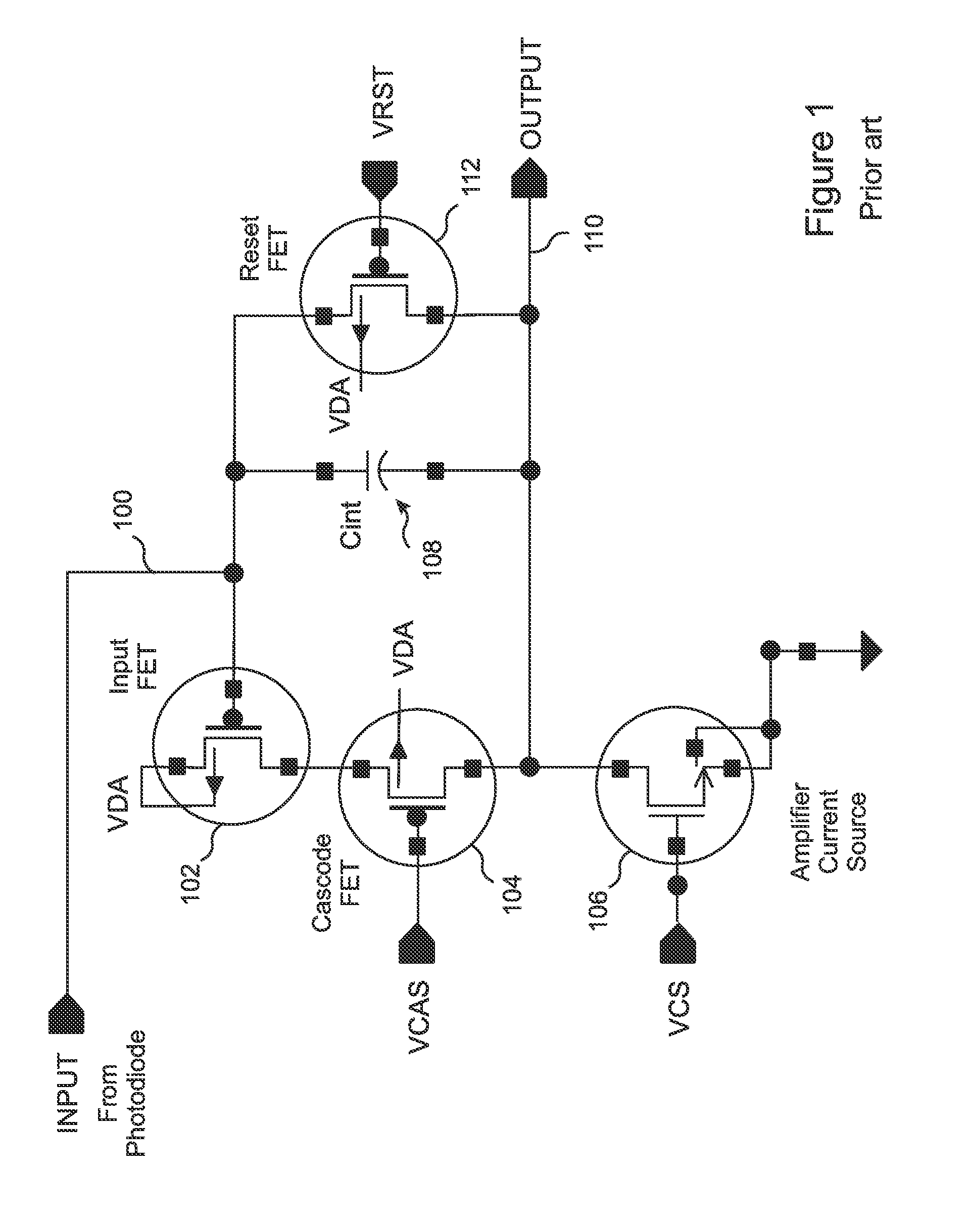
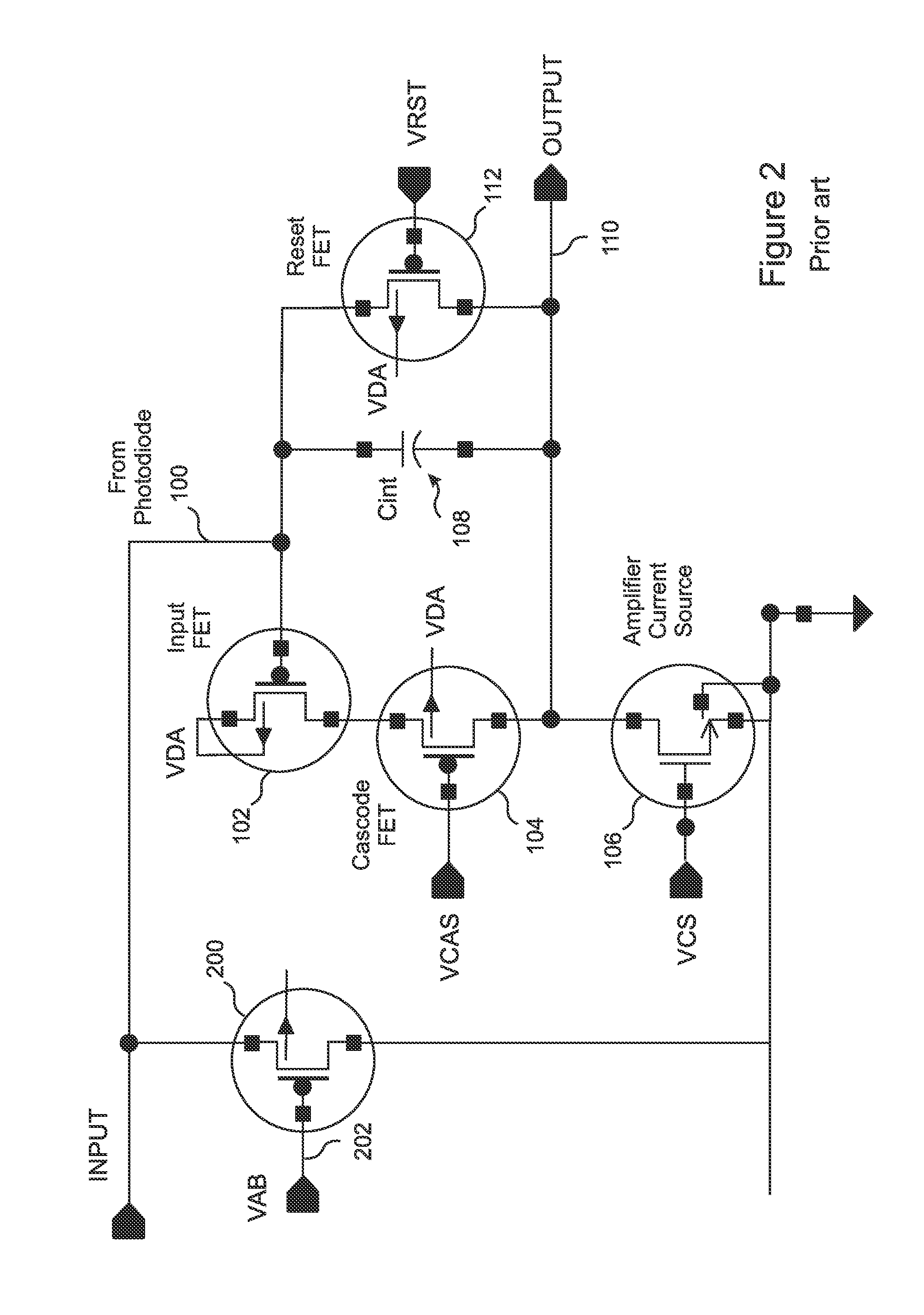
Instead, it will typically increase its conductance over some range of input voltages, and may never fully clamp the photodiode output voltage.
However, this can lead to added cost, added power consumption, and added space requirements.
While this may prevent blooming with moderate overloads, the voltage increase is likely large enough to cause significant integrating amplifier operating point changes, with a possible long recovery time following the removal of the overload.
Thus the degree of overload and anti-blooming protection afforded by prior art clamping circuits such as the one shown in FIG. 2 is, at best, limited and uncertain.
In effect, this approach does not prevent preamplifier overload, but functions only as an overload damage-control circuit that attempts to limit the propagation of deleterious overload effects to other photo-sensor circuits, and which in some cases is largely ineffective.
However, this approach may require the preamplifier output drive capability to exceed the maximum overload current delivered to the preamplifier input, a condition that the preamplifier may not be able to meet, at least not without an increase in preamplifier complexity.

Method used


Image

  • Anti-blooming circuit for integrating photodiode pre-amplifiers
  • Anti-blooming circuit for integrating photodiode pre-amplifiers
  • Anti-blooming circuit for integrating photodiode pre-amplifiers

Examples


Embodiment Construction

[0031]The present invention is a preamplifier input clamping circuit that maximizes performance while minimizing complexity, space, and cost. An embodiment of the invention is illustrated in FIG. 3. A clamping transistor 300, typically a clamping FET 300, is gated by the drain voltage of the input transistor 100 of the preamplifier, which is typically an input FET 100. The invention capitalizes on the fact that the initial effect of an input overload on a photo-sensor preamplifier is that its input transistor 100 is turned off, and its drain voltage will thereby go toward ground. Accordingly, the clamping transistor 300 is activated automatically and immediately when the input transistor 100 begins to turn off. It is not necessary to provide or to adjust a separate anti-blooming reference voltage 202.

[0032]The clamping behavior is sharp and substantially complete, since the clamping transistor 300 is driven by the input transistor 100, and not by a static reference voltage 202.

[0033...


PUM


Abstract

An input clamping circuit of a photo detector preamplifier is activated when an input transistor is turned off by an input overload, and the drain voltage of the input transistor is pulled toward ground by a current source. Even with extreme overloads, the operating conditions (Vgs and Id) of the input transistor remain within normal range. During normal operation, the clamping circuit is biased completely off, and has essentially no effect on circuit performance. Since the input FET itself, rather than a separate device, detects the onset of an overload, significantly improved clamping performance is realized without adding additional circuit complexity. The input transistor can be a FET. The preamplifier can be a cascode preamplifier. The clamping circuit can include a clamping FET or other clamping transistor gated by the input transistor drain. In embodiments, the clamping circuit increases current requirements of the preamplifier by no more than 25%.

Description

RELATED APPLICATIONS[0001]This application claims the benefit of U.S. Provisional Application No. 61 / 638,221, filed Apr. 25, 2012, which is herein incorporated by reference in its entirety for all purposes.STATEMENT OF GOVERNMENT INTEREST[0002]This invention was made with United States Government support under Contract No. FA9453-07-C-0181 awarded by U.S. Department of the Air Force. The United States Government has certain rights in this invention.FIELD OF THE INVENTION[0003]The invention relates to optical sensing apparatus, and more particularly, to circuitry that minimizes the effect of a very large optical input on an optical sensing apparatus.BACKGROUND OF THE INVENTION[0004]Arrays of photo-sensors, typically arrays of photo diodes, are well known and in wide use for many applications, such as the capture of images by digital cameras and digital video recorders. When an image is focused by a lens onto such an array, it is often referred to as a Focal Planar Array, or “FPA.” Th...

Claims


Application Information

Patent Timeline
Patent Type & Authority Patents(United States)
IPC IPC(8): H03F3/08
CPCH03F3/082
Inventor MADISON, GARY, M
Owner BAE SYST INFORMATION & ELECTRONICS SYST INTEGRATION INC
Learn More