
Conductive sheet, method for using conductive sheet, and touch panel

a technology of conductive sheets and touch panels, applied in the direction of electronic switching, pulse techniques, instruments, etc., can solve the problems of transparency and visibility of the electric motor, and achieve the effect of lowering resistance, improving visibility, and lowering resistan

Inactive Publication Date: 2014-12-23
FUJIFILM CORP
View PDF20 Cites 12 Cited by
  • Summary
  • Abstract
  • Description
  • Claims
  • Application Information

AI Technical Summary

Benefits of technology

The present invention provides a conductive sheet and a touch panel that have a conductive pattern with lowered resistance and improved visibility. The conductive sheet can be used in a projected capacitive touch panel. Additionally, the method described in the patent can create a conductive pattern that has better performance than existing technologies. This allows for the creation of larger touch panels with lower resistance and improved visibility.

Problems solved by technology

However, in the case of using the thin metal wires for the electrode, the thin metal wires are composed of an opaque material, whereby the electrode has problems of transparency and visibility.

Method used


Image

  • Conductive sheet, method for using conductive sheet, and touch panel
  • Conductive sheet, method for using conductive sheet, and touch panel
  • Conductive sheet, method for using conductive sheet, and touch panel

Examples


examples

[0306]The present invention will be described more specifically below with reference to Examples. Materials, amounts, ratios, treatment contents, treatment procedures, and the like, used in Examples, may be appropriately changed without departing from the scope of the invention. The following specific examples are therefore to be considered in all respects as illustrative and not restrictive.

first example

[0307]The surface resistance and the transmittance of each conductive sheet according to Examples 1 to 8 and Reference Examples 1 and 2 were measured, and the moire and the visibility were evaluated.

examples 1 to 8 and reference examples 1 and 2

Photosensitive Silver Halide Material

[0308]An emulsion containing an aqueous medium, a gelatin, and silver iodobromochloride particles was prepared. The amount of the gelatin was 10.0 g per 150 g of Ag, and the silver iodobromochloride particles had an I content of 0.2 mol %, a Br content of 40 mol %, and an average spherical equivalent diameter of 0.1 μm.

[0309]K3Rh2Br9 and K2IrCl6 were added to the emulsion at a concentration of 10−7 mol / mol-silver to dope the silver bromide particles with Rh and Ir ions. Na2PdCl4 was further added to the emulsion, and the resultant emulsion was subjected to gold-sulfur sensitization using chlorauric acid and sodium thiosulfate. The emulsion and a gelatin hardener were applied to the first transparent substrate 14A and the second transparent substrate 14B composed of a polyethylene terephthalate (PET). The applied silver amount was 10 g / m2, and the Ag / gelatin volume ratio was 2 / 1.

[0310]The PET support had a width of 30 cm, and the emulsion was appl...


PUM


Abstract

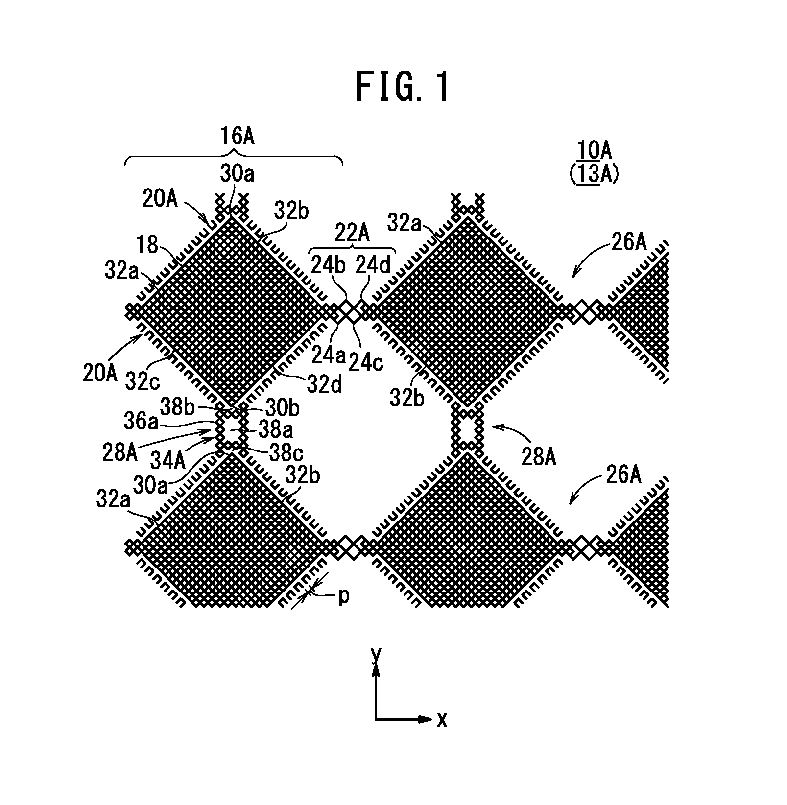
A conductive sheet, method for using conductive sheet and touch panel, having a base substance and conductive parts formed on one of the principal surfaces of the base substance. The conductive parts respectively extend in primary directions, and have two or more conductive patterns made from metal wires arranged in a second direction that is perpendicular to the first direction. The conductive pattern is constituted by serially connecting two or more large gratings in the first direction, and each of the large gratings is constituted by combining two or more small gratings. Around the edges of the large grating, non-connective patterns are formed from metal wires which are not connected with the large gratings.

Description

CROSS-REFERENCE TO RELATED APPLICATIONS[0001]The present invention is a 35 U.S.C. 371 National Stage Entry of PCT / JP2011 / 051692, filed Jan. 28, 2011, which claims priority from Japanese Patent Application Nos. 2010-017293, filed on Jan. 28, 2010, 2010-105865, filed on Apr. 30, 2010, 2010-153232, filed on Jul. 5, 2010, and 2010-281465, filed on Dec. 17, 2010, the contents of all of which are herein incorporated by reference in their entirety.TECHNICAL FIELD[0002]The present invention relates to a conductive sheet, a method for using a conductive sheet, and a touch panel, and for example to a conductive sheet suitable for use in a projected capacitive touch panel, a method for using a conductive sheet, and a touch panel.BACKGROUND ART[0003]Touch panels have attracted much attention in recent years. For example, a touch panel, which uses ITO (indium tin oxide) as an electrode material to form a less-visible electrode matrix, has been disclosed (see, Japanese Laid-Open Patent Publicatio...

Claims


Application Information

Patent Timeline
Patent Type & Authority Patents(United States)
IPC IPC(8): G06F3/044G06F3/041
CPCG06F3/044G06F2203/04112G06F2203/04103H03K2017/9613G06F3/047H03K2217/960755H03K17/9622G06F3/0412G06F3/0445G06F3/0446
Inventor KURIKI, TADASHI
Owner FUJIFILM CORP
Learn More