Display device and electronic device including display device
a technology of electronic devices and display devices, which is applied in the direction of semiconductor devices, electrical devices, instruments, etc., can solve the problems of increasing power consumption of display devices and reducing the aperture ratio of pixels, so as to reduce the driving voltage of light-emitting elements, increase the aperture ratio, and increase the aperture ratio
- Summary
- Abstract
- Description
- Claims
- Application Information
AI Technical Summary
Benefits of technology
Problems solved by technology
Method used
Image

Examples
embodiment 1
(Embodiment 1)
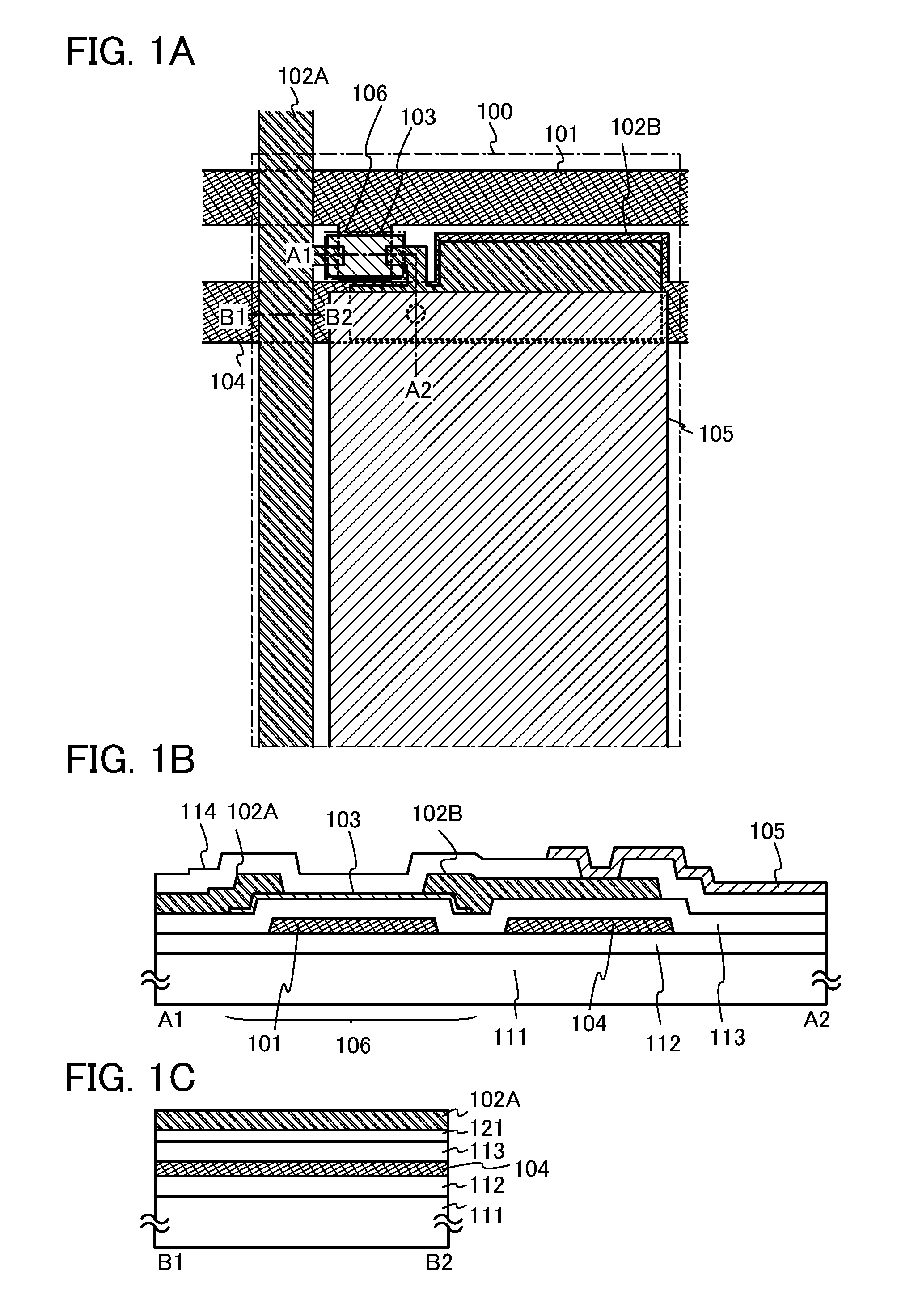
[0070]In this embodiment, an example of a pixel including a thin film transistor in which a highly-purified oxide semiconductor is used and a pixel electrode will be described below with reference to FIGS. 1A to 1C, FIG. 2, FIG. 3, and FIGS. 4A and 4B.
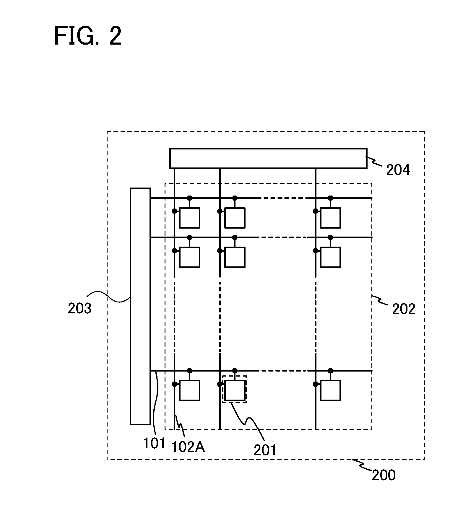
[0071]First, FIG. 1A is a top view of the pixel. Note that as an example of a structure of a TFT illustrated in FIG. 1A, a bottom gate structure that is a so-called inverted staggered structure is illustrated, in which wiring layers that serve as source and drain electrodes of a TFT are provided on one side of an oxide semiconductor layer that serves as a channel region, and a wiring that serves as a gate is provided on the other side of the oxide semiconductor layer. A pixel 100 illustrated in FIG. 1A includes a first wiring 101 that functions as a scan line, a second wiring 102A that functions as a signal line, an oxide semiconductor layer 103, a capacitor line 104, and a pixel electrode 105, and in addition to the abov...
embodiment 2
(Embodiment 2)
[0120]In this embodiment, an example of a thin film transistor that can be applied to the display device disclosed in this specification will be described. A thin film transistor 410 described in this embodiment can be used as the thin film transistor 106 in Embodiment 1.
[0121]An embodiment of a thin film transistor of this embodiment and an embodiment of a method for manufacturing the thin film transistor will be described with reference to FIGS. 5A and 5B and FIGS. 6A to 6E.
[0122]FIG. 5A illustrates an example of a top surface structure of a thin film transistor and FIG. 5B illustrates an example of a cross-sectional structure thereof. The thin film transistor 410 illustrated in FIGS. 5A and 5B is a top-gate thin film transistor.
[0123]FIG. 5A is a top view of the top-gate thin film transistor 410 and FIG. 5B is a cross-sectional view taken along line C1-C2 in FIG. 5A.
[0124]The thin film transistor 410 includes, over a substrate 400 having an insulating surface, an in...
embodiment 3
(Embodiment 3)
[0204]In this embodiment, an example of a thin film transistor that can be applied to the display device disclosed in this specification will be described. Note that for portions that are the same as those in Embodiment 2 and portions and steps that are similar to those in Embodiment 2, Embodiment 2 can be referred to, and description thereof is not repeated. In addition, detailed description of the same parts is omitted. A thin film transistor 460 described in this embodiment can be used as the thin film transistor 106 in Embodiment 1.
[0205]An embodiment of a thin film transistor of this embodiment and an embodiment of a method for manufacturing the thin film transistor will be described with reference to FIGS. 7A and 7B and FIGS. 8A to 8E.
[0206]FIG. 7A illustrates an example of a top surface structure of a thin film transistor and FIG. 7B illustrates an example of a cross-sectional structure thereof. The thin film transistor 460 illustrated in FIGS. 7A and 7B is a to...
PUM
 Abstract
Description
Claims
Application Information
 - R&D
- Intellectual Property
- Life Sciences
- Materials
- Tech Scout
- Unparalleled Data Quality
- Higher Quality Content
- 60% Fewer Hallucinations
Browse by: Latest US Patents, China's latest patents, Technical Efficacy Thesaurus, Application Domain, Technology Topic, Popular Technical Reports.
© 2025 PatSnap. All rights reserved.Legal|Privacy policy|Modern Slavery Act Transparency Statement|Sitemap|About US| Contact US: help@patsnap.com