Semiconductor device
a semiconductor device and semiconductor technology, applied in the direction of semiconductor devices, electrical equipment, transistors, etc., can solve the problems of reducing the threshold voltage of the transistor in the negative direction, difficult to and the malfunction of the semiconductor device, so as to reduce the carrier, suppress the release of oxygen from the n-type oxide semiconductor film, and reduce the carrier
- Summary
- Abstract
- Description
- Claims
- Application Information
AI Technical Summary
Benefits of technology
Problems solved by technology
Method used
Image

Examples
embodiment 1
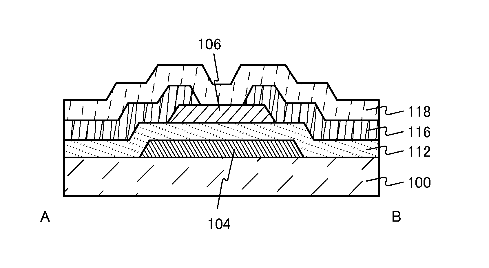
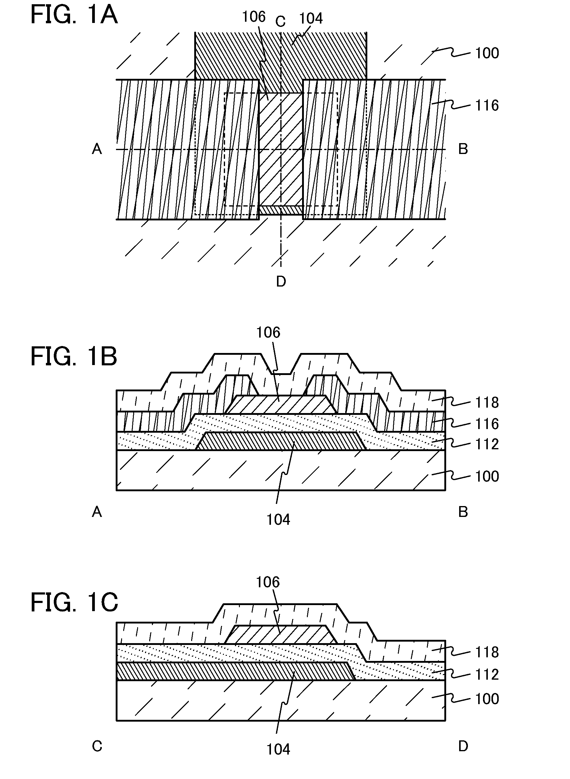
[0041]In this embodiment, an example of a transistor according to an embodiment of the present invention will be described with reference to FIGS. 1A to 1C.
[0042]FIG. 1A is a top view of the transistor. A cross section along dashed-dotted line A-B in FIG. 1A and a cross section along dashed-dotted line C-D in FIG. 1A correspond to a cross section A-B in FIG. 1B and a cross section C-D in FIG. 1C, respectively.
[0043]Here, the cross section A-B in FIG. 1B will be described in detail.
[0044]The transistor illustrated in FIG. 1B includes a gate electrode 104 over a substrate 100, a gate insulating film 112 covering the gate electrode 104, an oxide semiconductor film 106 over the gate electrode 104 with the gate insulating film 112 interposed therebetween, a pair of electrodes 116 which are over the oxide semiconductor film 106 and partly in contact with the oxide semiconductor film 106, and an interlayer insulating film 118 covering the gate insulating film 112, the oxide semiconductor f...
embodiment 2
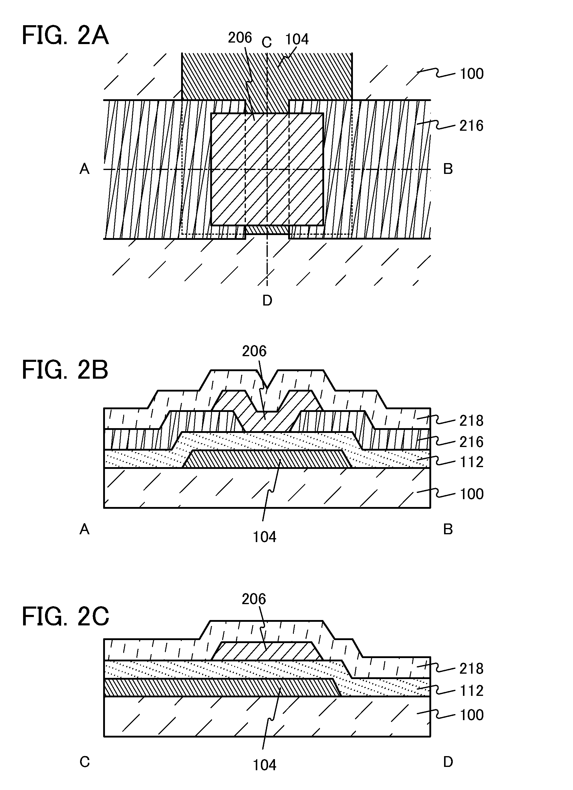
[0082]In this embodiment, a transistor having a structure different from that of the transistor described in Embodiment 1 will be described.
[0083]FIGS. 2A to 2C are a top view and cross-sectional views of a transistor according to an embodiment of the present invention. A cross section along dashed-dotted line A-B in FIG. 2A and a cross section along dashed-dotted line C-D in FIG. 2A correspond to a cross section A-B in FIG. 2B and a cross section C-D in FIG. 2C, respectively.
[0084]The cross section A-B in FIG. 2B will be described in detail below.
[0085]The transistor illustrated in FIG. 2B includes a gate electrode 104 over a substrate 100, a gate insulating film 112 covering the gate electrode 104, a pair of electrodes 216 over the gate insulating film 112, an oxide semiconductor film 206 which is over the pair of electrodes 216 and partly in contact with the pair of electrodes 216, and an interlayer insulating film 218 covering the gate insulating film 112, the pair of electrodes...
embodiment 3
[0107]In this embodiment, a liquid crystal display device manufactured using the transistor described in Embodiment 1 or 2 will be described. Note that although an example in which an embodiment of the present invention is applied to the liquid crystal display device is described in this embodiment, the present invention is not limited thereto. For example, application of an embodiment of the present invention to an electroluminescence (EL) display device is readily conceived by those skilled in the art.
[0108]FIG. 7 is a circuit diagram of an active matrix liquid crystal display device. The liquid crystal display device includes source lines SL_1 to SL_a, gate lines GL_1 to GL_b, and a plurality of pixels 200. Each pixel 200 includes a transistor 230, a capacitor 220, and a liquid crystal element 210. A plurality of the pixels 200 with such a structure form a pixel portion of the liquid crystal display device. In the case where the source line or the gate line is simply mentioned, i...
PUM
 Abstract
Description
Claims
Application Information
 - R&D
- Intellectual Property
- Life Sciences
- Materials
- Tech Scout
- Unparalleled Data Quality
- Higher Quality Content
- 60% Fewer Hallucinations
Browse by: Latest US Patents, China's latest patents, Technical Efficacy Thesaurus, Application Domain, Technology Topic, Popular Technical Reports.
© 2025 PatSnap. All rights reserved.Legal|Privacy policy|Modern Slavery Act Transparency Statement|Sitemap|About US| Contact US: help@patsnap.com