Semiconductor device and method for operating the same

a technology of semiconductor devices and semiconductors, applied in the direction of mechanical actuation of burglar alarms, instruments, electric signalling details, etc., can solve the problems of inability to achieve excellent transmission and reception, inability to check the remaining charge of the battery or the operation of replacing the battery, and difficulty in realizing the excellent state of transmission and reception. , the effect of reducing the current and improving the reliability of the transistor

Active Publication Date: 2014-10-07
SEMICON ENERGY LAB CO LTD
View PDF33 Cites 4 Cited by
  • Summary
  • Abstract
  • Description
  • Claims
  • Application Information

AI Technical Summary

Benefits of technology

[0008]In view of the foregoing problems, it is an object of the invention to provide a semiconductor device including an RFID which can transmit and receive individual information without checking of the remaining charge of a battery or a replacing operation of the battery in accordance with deterioration over time of the battery for driving, and can maintain an excellent state for transmission and reception of individual information even when the power of the radio wave or the electromagnetic wave (the carrier wave) from outside is insufficient.
[0019]Note that a switch described in the invention can employ an electrical switch, or a mechanical switch, for example. That is, any element can be employed as long as it can control a current flow, and thus, a switch is not limited to a certain element. For example, it may be a transistor, a diode (e.g., a PN junction diode, a PIN diode, a Schottky diode, or a diode-connected transistor), or a logic circuit combining such elements. Therefore, in the case of employing a transistor as a switch, the polarity (conductivity type) of the transistor is not particularly limited to a certain type since it operates just as a switch. However, when off-current is preferred to be small, a transistor of the polarity with smaller off-current is preferably employed. A transistor provided with an LDD region, a transistor with a multi-gate structure, or the like is given as an example of a transistor with small off-current. In addition, it is preferable that an n-channel transistor be employed when a potential of a source terminal of the transistor which is operated as a switch is closer to a low-potential-side power supply (e.g., Vss, GND, or 0 V), while a p-channel transistor be employed when the potential of the source terminal is closer to a high-potential-side power supply (e.g., Vdd). This is because the absolute value of a gate-source voltage of the transistor can be increased, so that the transistor can easily function as the switch. Note that a CMOS switch may also be employed by using both n-channel and p-channel transistors. By employing the CMOS switch, the switch can be operated appropriately even in the case in which a condition is changed such that a voltage output through the switch (in other words, a voltage input into the switch) is higher or lower than a voltage of output side.
[0022]The structure of a transistor can be various modes without limiting to a certain structure. For example, a multi-gate structure having two or more gate electrodes may be used. By using the multi-gate structure, off-current can be reduced and the withstand voltage can be increased to improve reliability of the transistor, or even if a drain-source voltage fluctuates when the transistor operates in a saturation region, flat characteristics can be provided without causing fluctuations of drain-source current very much. In addition, a structure where gate electrodes are formed above and below a channel may be used. By using the structure where gate electrodes are formed above and below the channel, a channel region is enlarged to increase the amount of current flowing therethrough, or a depletion layer can be easily formed to decrease the S value. In addition, a structure where a gate electrode is formed over a channel, a structure where a gate electrode is formed below a channel, a staggered structure, an inversely staggered structure, a structure where a channel region is divided into a plurality of regions and divided regions are connected in parallel or in series may be employed. A source electrode or a drain electrode may overlap with a channel (or a part of it). By employing the structure where the source electrode or the drain electrode may overlap with the channel (or the part of it), the case where an electric charge is accumulated in the part of the channel so that an operation becomes unstable can be prevented. In addition, a LDD (Lightly Doped Drain) region may be provided. By providing the LDD region, off-current can be reduced and the withstand voltage can be increased to improve reliability of the transistor, or even if a drain-source voltage fluctuates when the transistor operates in a saturation region, flat characteristics can be provided without causing fluctuations of drain-source current very much.
[0023]Note that as described above, various types of transistors may be employed as the transistor in the invention, and such transistors can be formed over various types of substrates. Accordingly, all of circuits may be formed over a glass substrate, a plastic substrate, a single crystalline substrate, an SOI substrate, or any other substrates. By forming all of the circuits over the same substrate, the number of component parts can be reduced to cut cost, or the number of connections to the circuit components can be reduced to improve reliability. Alternatively, parts of the circuits may be formed over one substrate and the other parts of the circuits may be formed over another substrate. That is, not all of the circuits are required to be formed over the same substrate. For example, parts of the circuits may be formed with transistors over a glass substrate and the other parts of the circuits may be formed over a single crystalline substrate (IC chip), so that the IC chip may be connected to the glass substrate by COG (Chip On Glass). Alternatively, the IC chip may be connected to the glass substrate by TAB (Tape Automated Bonding) or a printed wiring board. In this manner, by forming parts of the circuits over the same substrate, the number of component parts can be reduced to cut cost, or the number of connections to the circuit components can be reduced to improve the reliability. In addition, by forming a portion with a high driving voltage or a portion with high driving frequency which would consume large power over another substrate, increase of power consumption can be prevented.
[0025]A semiconductor device of the invention includes a battery. Therefore, unlike a conventional technique, shortage of power for transmission and reception of individual information in accordance with deterioration over time of the battery can be prevented. The battery can be charged by utilizing power of a radio wave or an electromagnetic wave from outside without being connected to a battery charger. Accordingly, the battery can be sequentially used without the need of checking of the remaining charge of the battery or an operation of replacing the battery unlike an active-type RFID. In addition, power for driving an RFID is always held in the battery so that sufficient power for driving the RFID can be obtained; therefore, communication distance from a reader / writer can be increased.

Problems solved by technology

Thus, there is a problem in that power which is necessary for transmission and reception of individual information cannot be finally obtained from the battery.
Therefore, in order to sequentially use the active-type RFID having the battery for driving, there is a problem in that checking of the remaining charge of the battery or an operation of replacing the battery is needed.
In addition, as shown in FIG. 2, in the case of a passive-type RFID in which a power supply for driving is generated by utilizing power of a radio wave or an electromagnetic wave (a carrier wave) from outside, there is a problem in that transmission and reception of a signal from long distance and securing of power for transmitting a radio wave which is necessary for transmission and reception are difficult, so that an excellent state for transmission and reception is difficult to be realized.
Therefore, in order to use the passive-type RFID in which the power supply for driving is generated by utilizing the power of the radio wave or the electromagnetic wave (the carrier wave) from outside, there is a problem in that the use of the semiconductor device is limited to short distance from an antenna of a reader / writer which is a unit for supplying power, in which supply of the power of the radio wave or the electromagnetic wave (the carrier wave) from outside is sufficient.

Method used


Image

  • Semiconductor device and method for operating the same
  • Semiconductor device and method for operating the same
  • Semiconductor device and method for operating the same

Examples


embodiment mode 1

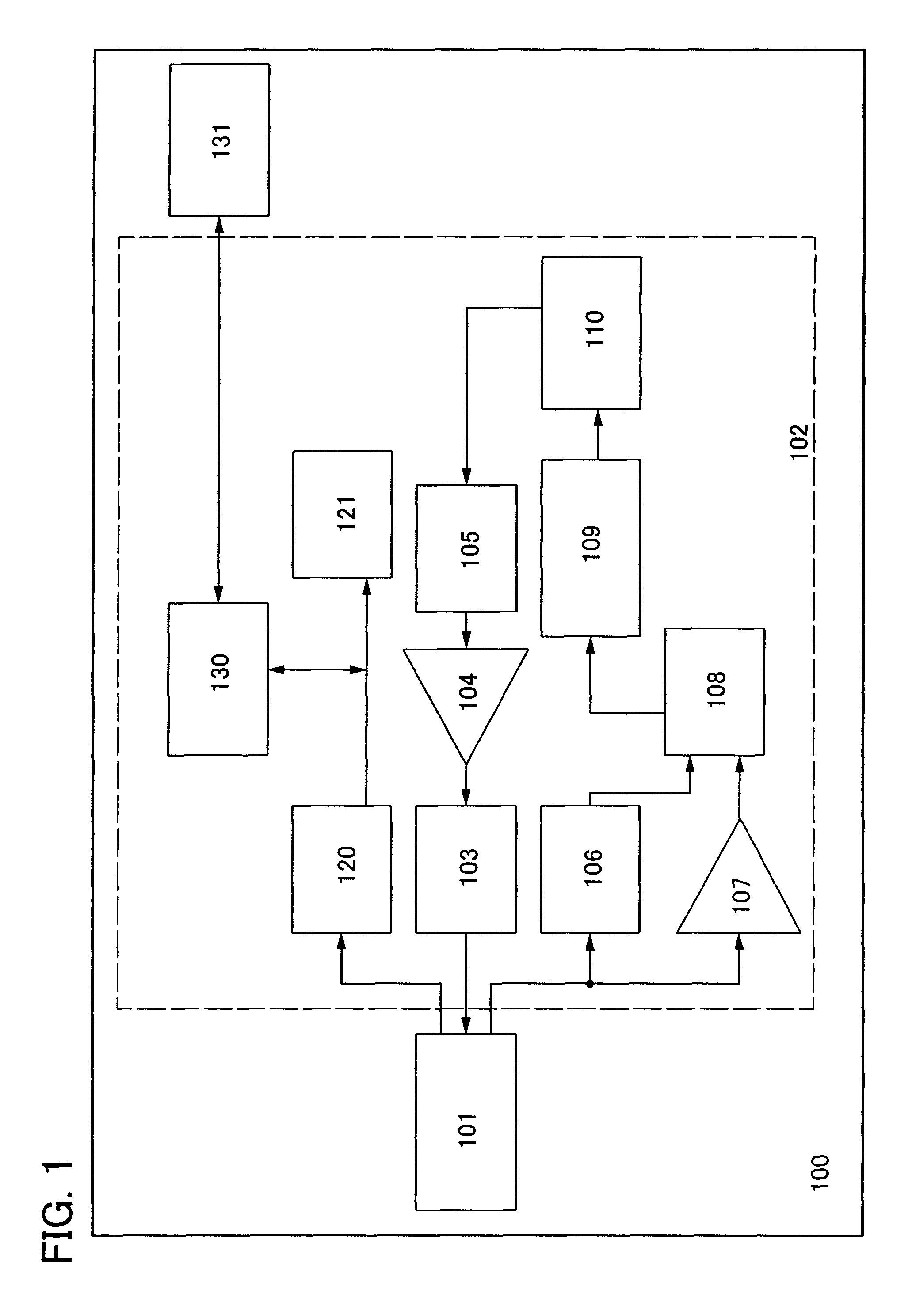
[0060]First, a schematic structure of a semiconductor device in accordance with Embodiment Mode 1 of the invention is briefly described.

[0061]The semiconductor device includes an antenna circuit, a signal processing circuit which processes a signal received by the antenna circuit, and a battery which stores power supplied.

[0062]The antenna circuit includes an antenna which receives a signal.

[0063]As the shape of the antenna in the antenna circuit, various types can be employed. For example, the shape such as a so-called dipole antenna, a loop antenna, a Yagi antenna, a patch antenna, or a minute antenna can be employed. In the case where the antenna is formed over the substrate as a transistor included in the signal processing circuit, the shape of the antenna is preferably a minute loop antenna, a minute dipole antenna, or the like.

[0064]In addition, the antenna circuit may include a unit for changing the frequency of the signal received. For example, when the shape of the antenna ...

embodiment mode 2

[0109]In a semiconductor device in accordance with Embodiment Mode 2 of the invention, a structure in which the semiconductor device in accordance with Embodiment Mode 1 of the invention is provided with a so-called booster antenna is shown.

[0110]First, a schematic structure of the semiconductor device in accordance with Embodiment Mode 2 of the invention is briefly described.

[0111]The semiconductor device includes an antenna circuit, a signal processing circuit which processes a signal received by the antenna circuit, and a battery which stores power supplied.

[0112]Note that the antenna circuit includes a first antenna portion and a second antenna portion. The first antenna portion includes a first antenna coil and the second antenna portion includes a second antenna coil having a longer outside diameter than that of the first antenna coil. The transmission and reception frequency of the first antenna portion tunes to the transmission and reception frequency of the second antenna p...

embodiment mode 3

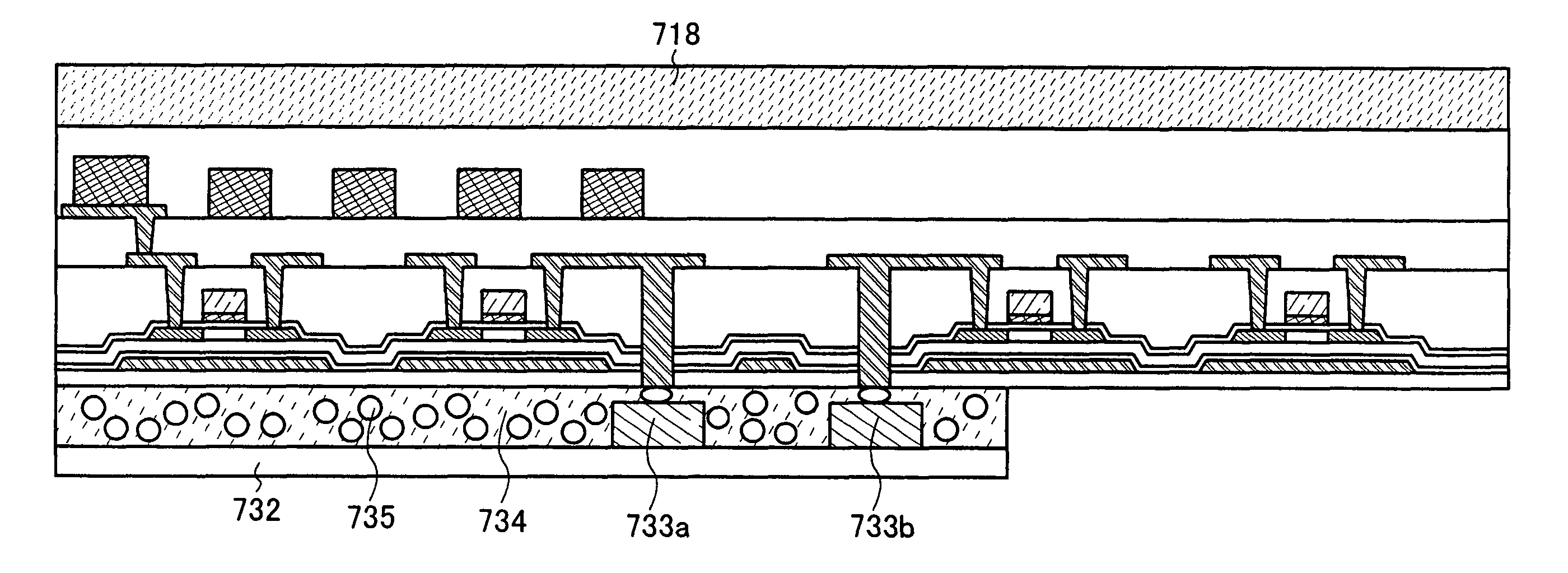
[0137]In this embodiment mode, an example of a manufacturing method of the semiconductor device shown in the aforementioned embodiment modes is described with reference to the drawings.

[0138]First, a release layer 603 is formed over one surface of a substrate 601 with an insulating film 602 interposed therebetween. Sequentially, an insulating film 604 functioning as a base film and a semiconductor film 605 (e.g., a film including amorphous silicon) are stacked (see FIG. 11A). Note that the insulating film 602, the release layer 603, the insulating film 604, and the amorphous semiconductor film 605 can be sequentially formed.

[0139]The substrate 601 is selected from a glass substrate, a quartz substrate, a metal substrate (e.g., a ceramic substrate or a stainless steel substrate), a semiconductor substrate such as a silicon substrate, or the like. In addition, a substrate made of polyethylene terephthalate (PET), polyethylene naphthalate (PEN), polyether sulfone (PES), acryl, or the l...


PUM


Abstract

To provide a semiconductor device including an RFID which can transmit and receive individual information without checking of the remaining charge of a battery or a replacing operation of the battery in accordance with deterioration over time of the battery for driving, and can maintain an excellent state for transmission and reception of individual information even when power of a radio wave or an electromagnetic wave from outside is insufficient. A battery (also described as a secondary battery) is provided as a power supply for supplying power to the RFID. Then, when power which is obtained from a signal received from outside is larger than predetermined power, its surplus power is stored in the battery; and when the power which is obtained from the signal received from outside is smaller than the predetermined power, power which is obtained from the battery is used for the power for driving.

Description

TECHNICAL FIELD[0001]The present invention relates to a semiconductor device. In particular, the invention relates to a semiconductor device which transmits and receives data through radio waves and receives power. In addition, the invention relates to a method for operating it. Further, the invention relates to a communication system which uses a semiconductor device using radio waves, an antenna and a reader / writer for transmitting and receiving data to / from the semiconductor device, and an antenna and a battery for supplying power to the semiconductor device.BACKGROUND ART[0002]In recent years, an individual identification technique utilizing radio communication such as radio waves or an electromagnetic waves has attracted attention. In particular, as a semiconductor device which communicates data by radio communication, an individual identification technique utilizing an RFID (Radio Frequency IDentification) tag has attracted attention. An RFID tag (hereinafter described simply ...

Claims


Application Information

Patent Timeline
Patent Type & Authority Patents(United States)
IPC IPC(8): H04Q5/22G06K19/07H01L21/768H01L23/522H01L23/532H01L29/417H01L29/423H01L29/49
CPCG06K19/0723G06K19/0701G06K19/0702H02J50/20
Inventor YAMAZAKI, SHUNPEIKOYAMA, JUNISHII, MASATOATSUMI, TOMOAKIOSADA, TAKESHIIKEDA, TAKAYUKIKUROKAWA, YOSHIYUKISHIONOIRI, YUTAKA
Owner SEMICON ENERGY LAB CO LTD
Why Eureka
Try Eureka