
Thin film transistor array panel and method for repairing the same

a thin film transistor and array panel technology, applied in the field of thin film transistor substrate and a method for repairing the same, can solve the problems of increasing the voltage, causing the defective pixel of the corresponding pixel to be damaged, short circuit, etc., to prevent the generation of defective pixel, prevent static electricity damage, and repair the effect of easy

Active Publication Date: 2014-09-02
SAMSUNG DISPLAY CO LTD
View PDF25 Cites 12 Cited by
  • Summary
  • Abstract
  • Description
  • Claims
  • Application Information

AI Technical Summary

Benefits of technology

The solution effectively blocks externally transmitted static electricity, prevents pixel damage, and allows for easy repair of damaged wires, thereby minimizing defective pixel rates and extending the substrate's functionality.

Problems solved by technology

The inflow static electricity causes increase of a voltage in the portion where the static electricity exists even through the amount of static electricity is insignificant so that an element like a thin film transistor may be damaged or a wire may be short-circuited.
Such a failure causes the corresponding pixel to be defective; therefore, a repairing process should be performed.

Method used


Image

  • Thin film transistor array panel and method for repairing the same
  • Thin film transistor array panel and method for repairing the same
  • Thin film transistor array panel and method for repairing the same

Examples


Embodiment Construction

[0045]The present invention will be described more fully hereinafter with reference to the accompanying drawings, in which exemplary embodiments of the invention are shown. As those skilled in the art would realize, the described embodiments may be modified in various different ways, all without departing from the spirit or scope of the present invention.

[0046]The drawings and description are to be regarded as illustrative in nature and not restrictive. Like reference numerals designate like elements throughout the specification.

[0047]In addition, the size and thickness of each component shown in the drawings are arbitrarily shown for understanding and ease of description, but the present invention is not limited thereto.

[0048]In the drawings, the thickness of layers, films, panels, regions, etc., are exaggerated for clarity. In the drawings, for understanding and ease of description, the thickness of some layers and areas is exaggerated. It will be understood that when an element s...


PUM

PropertyMeasurementUnit
thicknessaaaaaaaaaa
conductiveaaaaaaaaaa
areaaaaaaaaaaa

Abstract

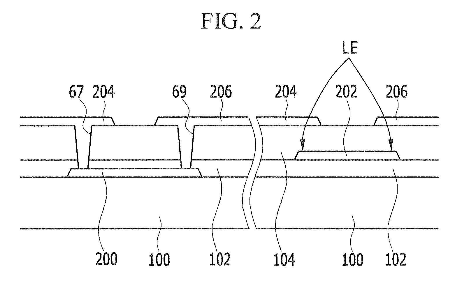
A thin film transistor substrate includes a substrate including a display area including: pixels and a periphery area where a driver for driving the pixels is disposed; first signal lines connected with the pixels and extended to the periphery area, and including first short-circuit portions provided in the periphery area; second signal lines connected with the pixels and extended to the periphery area by crossing the first signal lines in an insulated manner; first connection members overlapping lateral ends of the first signal lines, disposed in lateral sides with respect to the first short-circuited portions, and formed of a doped semiconductor; and first repairing conductors overlapping the lateral ends of the first signal lines, and disposed in the lateral sides with respect to the first short-circuited portions. Lateral ends of the first connection members are connected with the lateral ends of the first signal lines through contact holes.

Description

CLAIM OF PRIORITY[0001]This application makes reference to, incorporates the same herein, and claims all benefits accruing under 35 U.S.C. §119 from an application earlier filed in the Korean Intellectual Property Office on 19 Oct. 2012 and there duly assigned Serial No. 10-2012-0116738.BACKGROUND OF THE INVENTION[0002]1. Field of the Invention[0003]An embodiment of the present invention relates generally to a thin film transistor substrate and a method for repairing the same. More particularly, an embodiment of the present invention relates generally to a method for repairing damage due to static electricity.[0004]2. Description of the Related Art[0005]In general, a thin film transistor (TFT) array panel is used as a circuit board for independently driving each pixel in a liquid crystal display device, an organic electroluminescence (EL) display device, or the like. The thin film transistor substrate is formed of a scan signal wire transmitting a scan signal or a gate wire, an imag...

Claims


Application Information

Patent Timeline
Patent Type & Authority Patents(United States)
IPC IPC(8): G02F1/1345G02F1/00G02F1/1343
CPCG02F1/00G02F2001/134318H01L51/56H01L27/124H01L27/3248H01L21/76894H01L27/3276H10K59/123H01L27/0248H10K59/131H10K71/861G02F1/134318
Inventor JIN, GUANG-HAIKIM, DONG-GYUJUNG, KWAN-WOOKKIM, MOO-JIN
Owner SAMSUNG DISPLAY CO LTD
Learn More