Method of strain engineering and related optical device using a gallium and nitrogen containing active region

a technology of active region and strain engineering, which is applied in the direction of lasers, masers, semiconductor lasers, etc., can solve the problems of degrading the material characteristics of optical devices, affecting the operation of optical devices, so as to facilitate the manipulation of optical modes, efficient and reliable

Active Publication Date: 2014-08-26
KYOCERA SLD LASER INC
View PDF277 Cites 17 Cited by
  • Summary
  • Abstract
  • Description
  • Claims
  • Application Information

AI Technical Summary

Benefits of technology

The invention provides a method and device for emitting electromagnetic radiation using gallium and nitrogen containing materials such as gallium nitride. The invention includes a strain control region that allows for the integration of high indium content and thick InGaN regions without introducing defects to the surrounding areas. The strain control region facilitates the confinement of optical modes and manipulation of optical properties in devices such as laser diodes. The invention also provides a cost-effective optical device for laser applications that can be manufactured using conventional materials and methods. The invention can be used to control or engineer strain within the wave guiding layers and quantum well region of laser devices.

Problems solved by technology

Without inclusion of the strain control region, the cumulative strain becomes too great such that the epitaxial structure becomes heavily defected with dislocations and other lattice imperfections.
These defects degrade the material characteristics for use in optical devices, and they may exist at the interface between the high indium content and / or thick InGaN layer(s) and the underlying layer, and / or in the multi-quantum well active region, and / or in other regions.
Without the strain control region, the interface between the high indium content and / or thick layers of InGaN and the underlying layer becomes heavily defected and the multi-quantum well regions are significantly degraded with defects.
Further, as shown in the growth data and TEM images below, if the high indium content and / or thick InGaN layer exceeds some threshold value of strain, the multi-quantum well regions are plagued with defects.

Method used


Image

  • Method of strain engineering and related optical device using a gallium and nitrogen containing active region
  • Method of strain engineering and related optical device using a gallium and nitrogen containing active region
  • Method of strain engineering and related optical device using a gallium and nitrogen containing active region

Examples


Embodiment Construction

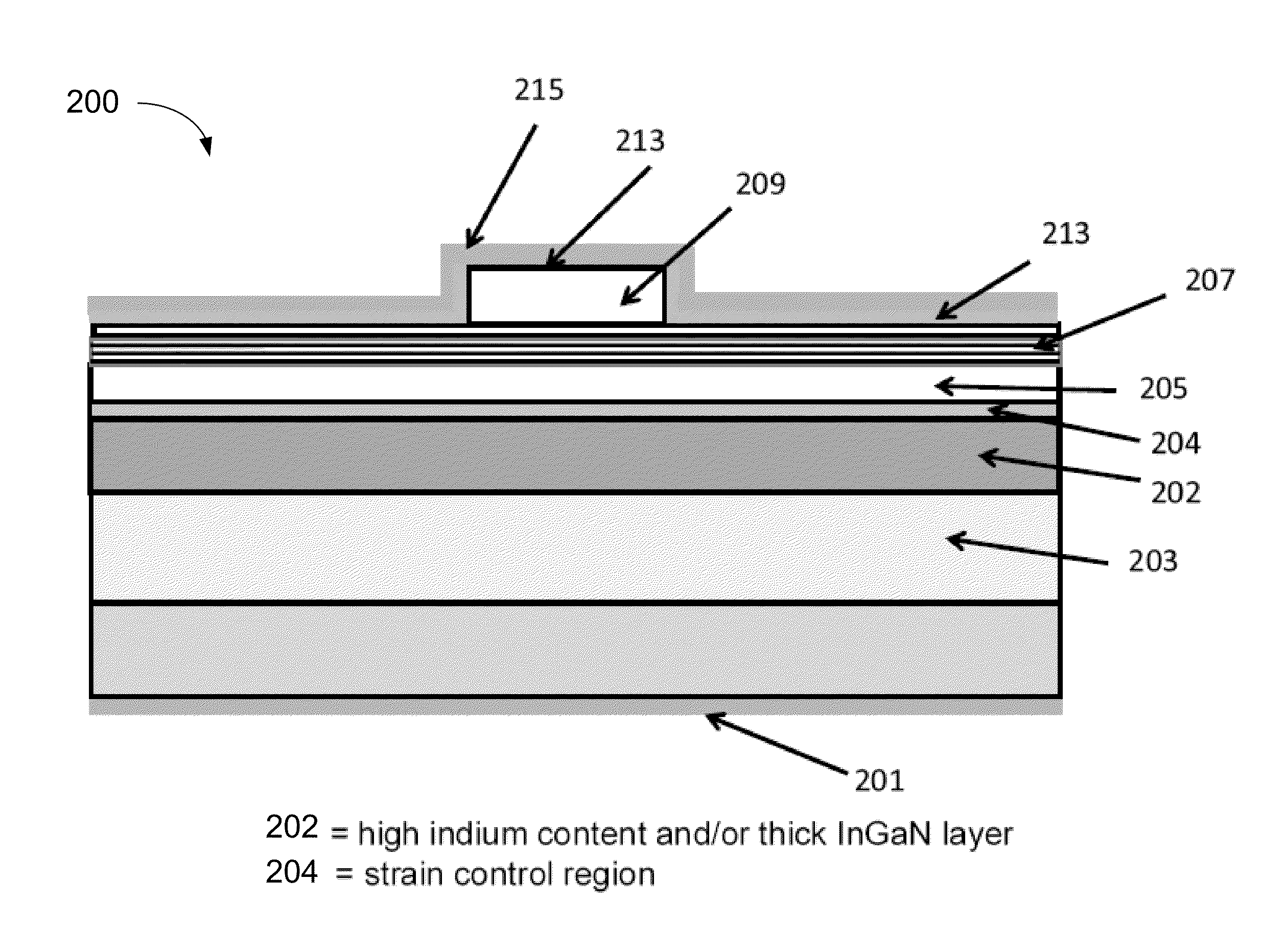
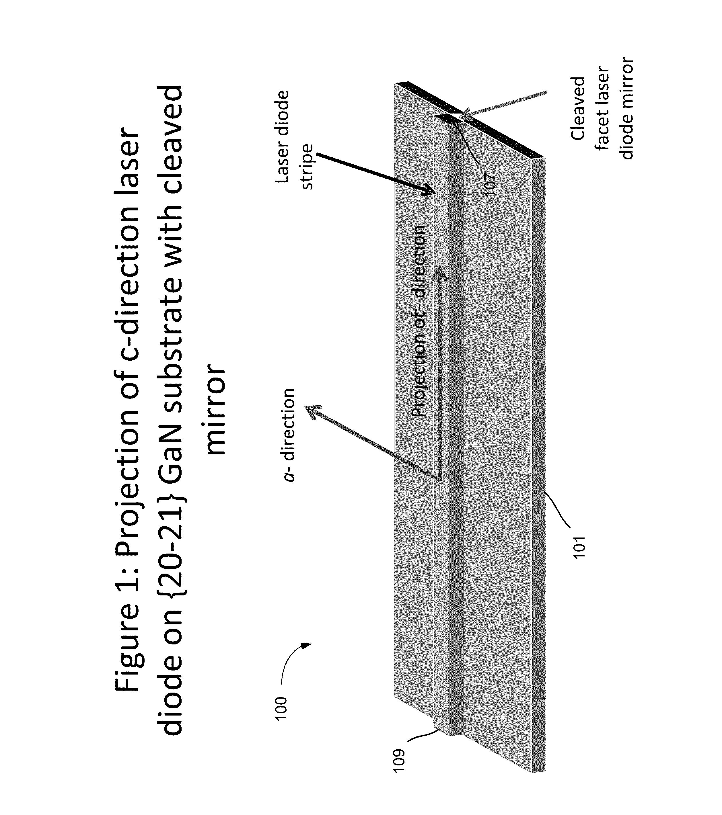
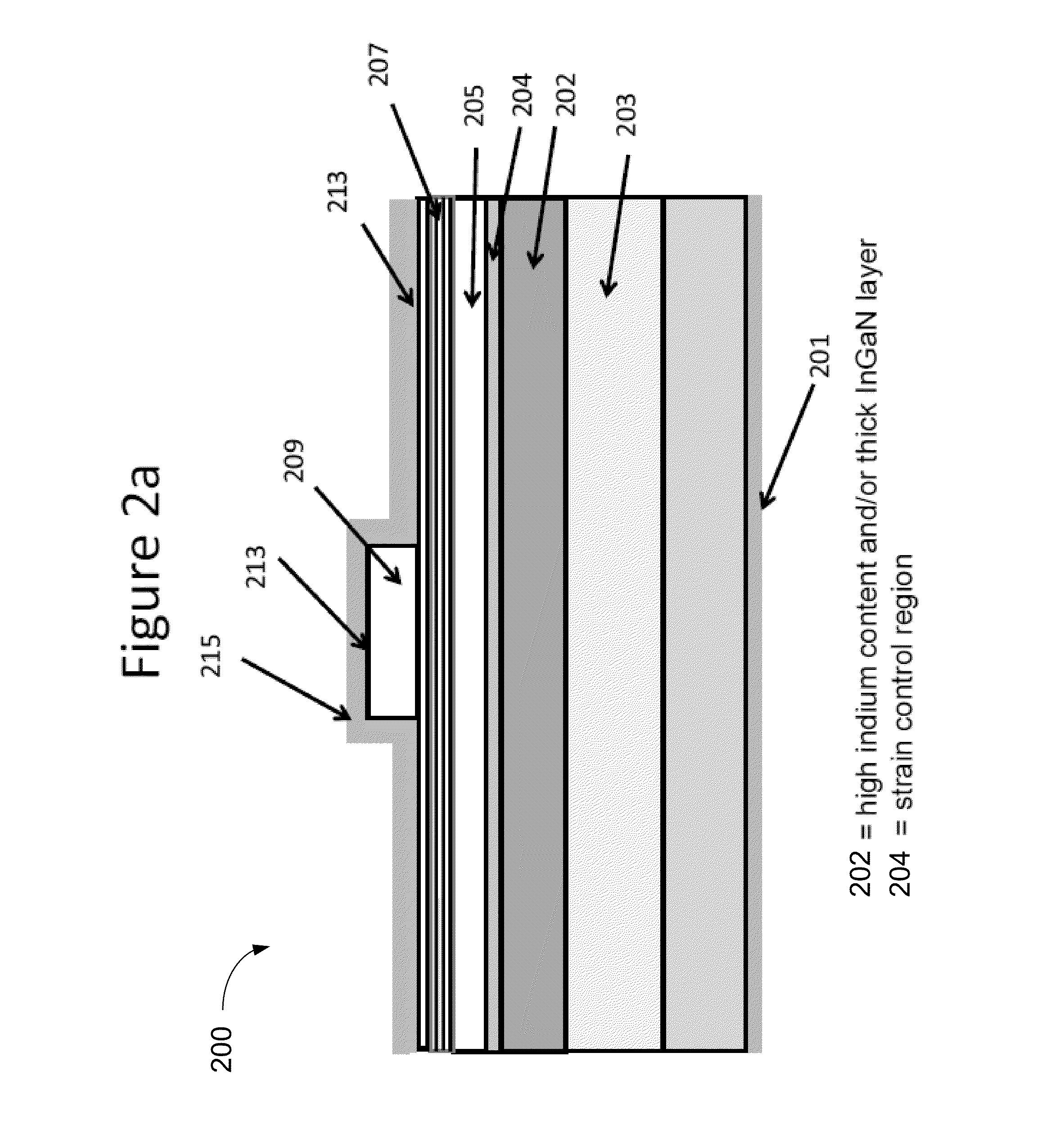
[0063]We have discovered a way to design and fabricate high intensity green laser diode devices in a specific embodiment. In a specific embodiment, the present method and structure includes a high indium content and / or thick InGaN layers in the present epitaxial structures grown on {20-21} and offcuts thereof in gallium and nitrogen containing substrates. In a preferred embodiment, the high indium content and / or thick InGaN layers include 200-300 nm InGaN layers with 6% indium, 100 nm InGaN layers with 10% indium, 60 nm InGaN layers with 13-15% indium, or 30 nm InGaN layers with 15-18% indium within the present green laser diode epitaxial structure without detriment to photoluminescence properties, electroluminescence properties, or defect density of the light emitting multiple quantum well active region. In a specific embodiment, the present green laser diode epitaxial structure includes an n-type GaN cladding region(s), an n-side separate confinement hetereostructure (SCH), a mult...


PUM


Abstract

An optical device has a gallium and nitrogen containing substrate including a surface region and a strain control region, the strain control region being configured to maintain a quantum well region within a predetermined strain state. The device also has a plurality of quantum well regions overlying the strain control region.

Description

CROSS REFERENCE TO RELATED APPLICATION[0001]This application claims priority to U.S. Provisional Application No. 61 / 410,794, filed Nov. 5, 2010, which is incorporated by reference in its entirety herein.BACKGROUND OF THE INVENTION[0002]The invention is directed to optical devices and related methods. In particular, the invention provides a method and device for emitting electromagnetic radiation using nonpolar or semipolar gallium containing substrates such as GaN, AN, InN, InGaN, AlGaN, and AlInGaN, and others. The invention provides a method and device using a gallium and nitrogen containing substrate configured on the {20-21} family of planes or an off-cut of the {20-21} family of planes towards the plus or minus c-plane and / or towards the a-plane according to one or more embodiments, but there can be other configurations. Still more particularly, the invention provides a method and resulting structures that use high indium content InGaN or thick InGaN regions to facilitate manip...

Claims


Application Information

Patent Timeline
Patent Type & Authority Patents(United States)
IPC IPC(8): H01L21/00
CPCH01L21/00H01L21/0254H01L33/00H01S1/00H01L21/02389H01L21/02433H01L21/02458H01L21/02507H01L21/0262H01S5/2009H01S5/2031H01S5/2201H01S5/3201H01S5/3202H01S5/3213H01S5/3063H01L33/16H01L33/32H01L33/06H01L33/12H01S5/34333H01S5/320275H01L33/0075H01S5/1082H01S5/3406H01S5/2018H01S5/34346H01S5/3403
Inventor RARING, JAMES W.POBLENZ, CHRISTIANE
Owner KYOCERA SLD LASER INC
Why Eureka
Try Eureka