Symmetric quadrupole structured field emission display without spacer

a structured field and display technology, applied in the field of fabrication techniques of field emission display, can solve the problems of limiting the use of high-voltage phosphors and the enhancement of lightness, poor gray-scale reproduction, and rapid aging of phosphors, and achieves low adjusting voltage, simple fabrication process, and new structure.

Active Publication Date: 2014-08-12
GUO TAILIANG +5
View PDF2 Cites 5 Cited by
  • Summary
  • Abstract
  • Description
  • Claims
  • Application Information

AI Technical Summary

Benefits of technology

[0012]The purpose of this invention is to provide a symmetric quadrupole structured field emission display without spacer, by overcoming the deficiencies of the existing technology. This field emitter is novel in structure, simple in fabrication process, low in adjusting voltage, and in favor for image uniformity and stable emission of electrons.
[0025]1. Simple fabrication process and low cost. It is needless of consideration for the fixation of spacers on the two substrates; the cathode and the gate are fabricated respectively on the upper substrate and the under substrate; it is also needless of fabrication of insulating dielectric layer between the anode and gate, since there are parallel without overlaps.
[0027]3. Low adjusting voltage, stable and reliable emission of electrons. Auxiliary electrodes are arranged side by side and alternating perpendicular on the top of the cathode on the under substrate, which can reduce the adjusting voltage of gate, avoid the charge accumulation, and collect the electrons from the cathode, improve the color purity and the emission rate of the electron. When fabricating the electron emitters using electrophoresis deposition, the auxiliary electrodes can control the orientation of the electron emitters, which can further improve the properties of field emission and the devices.

Problems solved by technology

However, the voltage of anode can not be too high as it is connected to the drive circuit, which limits the use of high voltage phosphors and the enhancement of the lightness, as well as poor gray-scale reproduction.
One need to increase the current density to maintain the high lightness, which will cause rapid aging of the phosphors, and decrease the lifetime of the devices.
Without limiting the driving voltage, it is more difficult to design the drive circuit, and difficult to achieve fast dynamic display with multi-gray scale.
Therefore, diode FED is limited in the practical application.
The cathode and the gate are perpendicularly aligned, with an insulating dielectric layer between the cathode and the gate to avoid the short circuit between the cathode and gate, the fabrication process is complicated and high costly.
Usually, the fabrication of the dielectric layer and gate is followed by that of the electronic materials, so the cathode materials subject to damage and contamination during the preparation of the dielectric layer and gate.
For this kind of FED, the leakage current of the insulating layer between cathode and gate is large, which will affect the lifetime of the device.
The cathode and the gate are perpendicularly aligned, with an insulating dielectric layer between the cathode and the gate to avoid the short circuit between the cathode and gate, the fabrication process is complicated and high costly.
However, it is easy to cause the short circuit between the cathode and the gate after the fabrication of emission materials on the cathodes.
However, there are some short cuts such as: charge accumulation, serious dispersion of electrons, lager beam spot, and crosstalk between the adjacent pixel units.
The crosstalk of the pixel unit can be reduced by narrowing the spacing of cathode and anode; however, it is not conducive to the increase of the anode voltage, leading to lower luminous efficiency.
The fabrication process is much simpler, however, it suffers a serious dispersion of electrons and lager beam spot, and need to use scan the high anode voltage to control the images.
The current technology is limited to fabricate the supporting structure alone; leading to the problems of distribution and placement of spacers.

Method used


Image

  • Symmetric quadrupole structured field emission display without spacer
  • Symmetric quadrupole structured field emission display without spacer
  • Symmetric quadrupole structured field emission display without spacer

Examples


Embodiment Construction

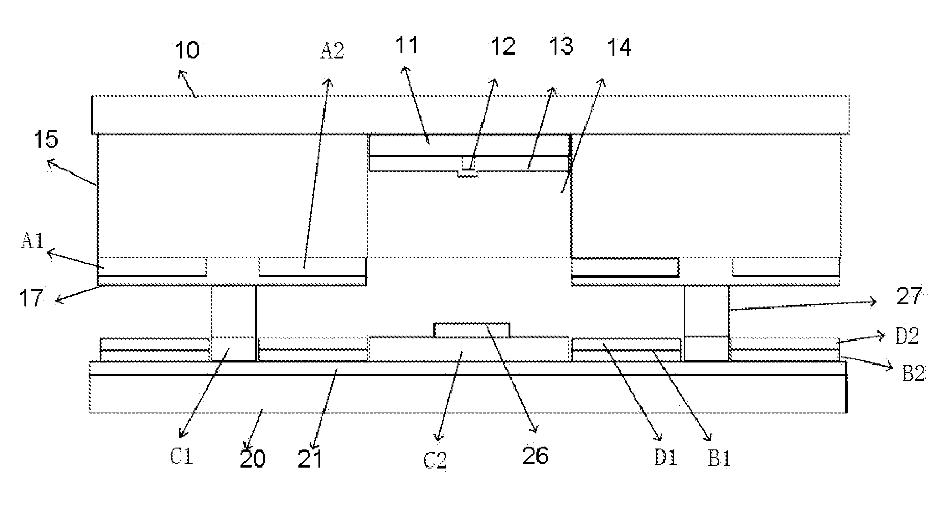
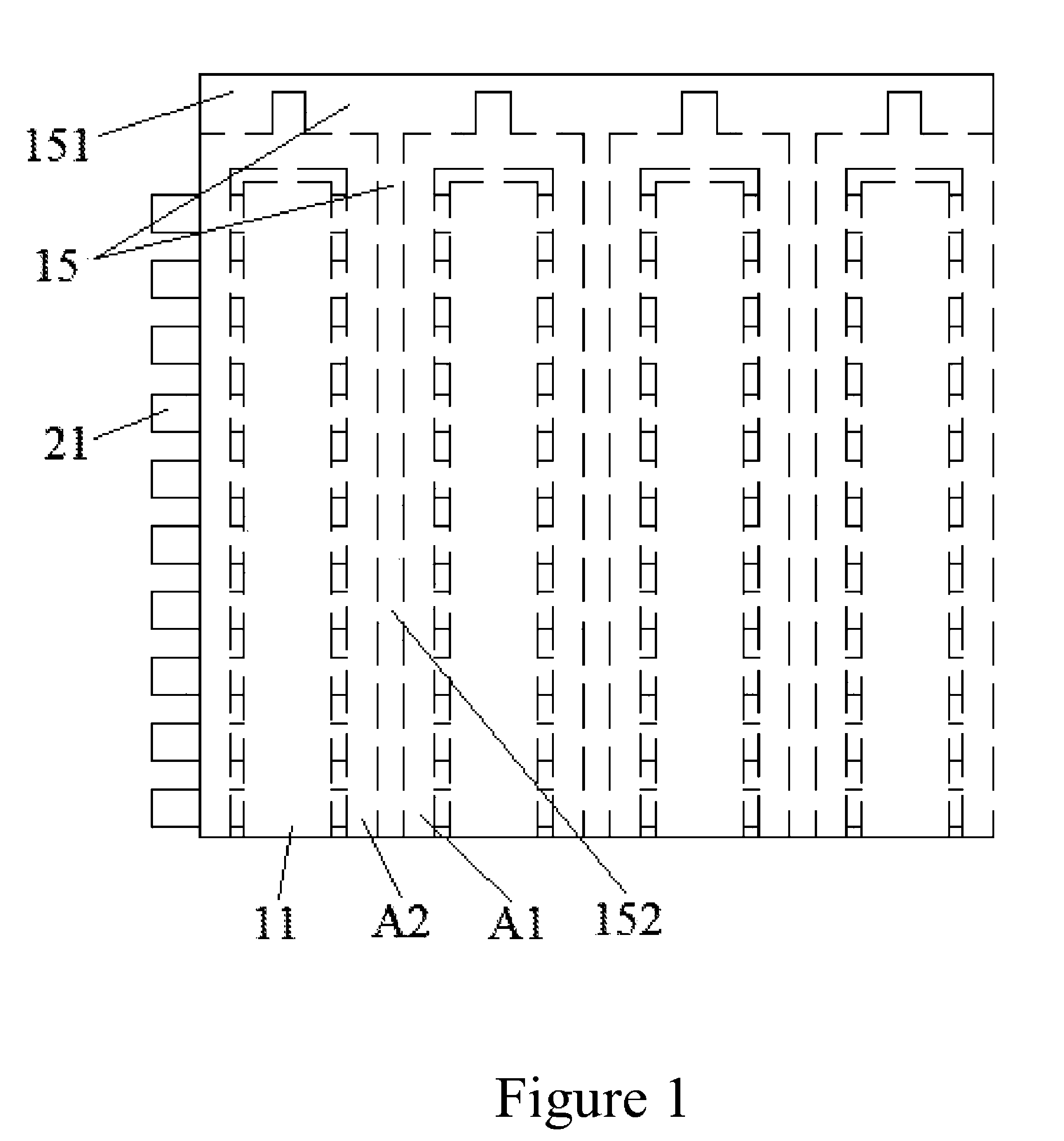
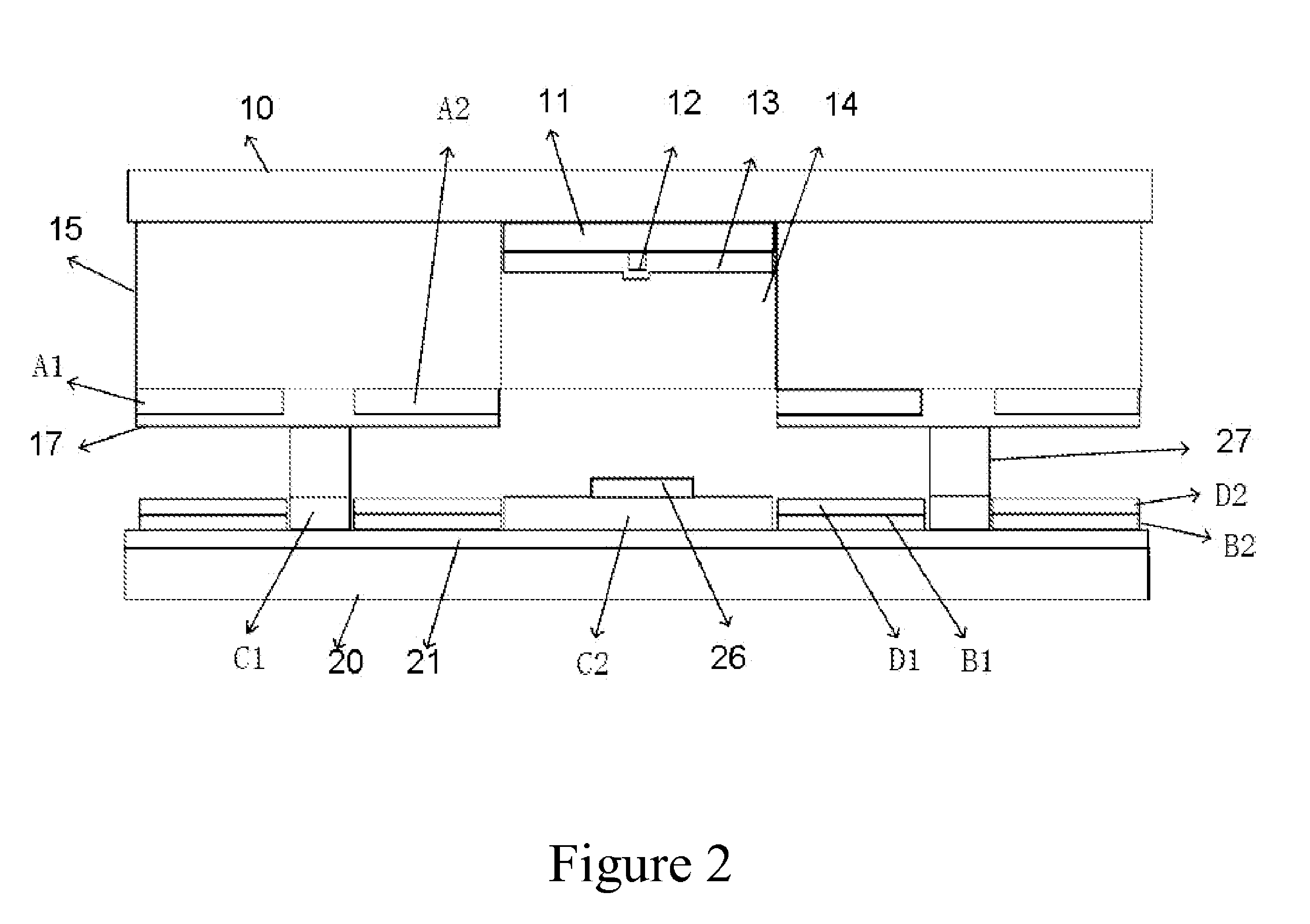
[0037]As shown in FIG. 1-4, the symmetric quadrupole structured field emission display without spacer, comprising two parallel substrates: upper substrate 10 and under substrate 20, which are adapted in the size, wherein a number of longitudinal strips of anode electrodes 11 are settled on the underside of the upper substrate 10 side by side, the bus electrodes 12 are settled on the anode 11 along the longitudinal centerline, phosphor layer 13 and anode dielectric layer 14 are settled on the anode 11 and bus electrode 12 along the longitudinal alternating, comb-like dielectric layer 15 is settled on the underside of the upper substrate 10, the comb-like dielectric layer 15 is composed of lateral connection belts 151 that are arranged in the flanking on the upper substrate 10 and a number of longitudinal work belts 152 that are arranged side by side on one side of the lateral connection belts 151, the longitudinal work belts 152 and the anodes 11 are parallel, and are arranged on the...


PUM


Abstract

The present invention relates to a symmetric quadrupole structured field emission display without spacer comprising the upper and under substrates with a dielectric layer in between, wherein comb-like dielectric layer with lateral connection belts and a number of longitudinal working belts and longitudinal anodes are arranged on the upper substrate, bus electrodes are arranged longitudinally along the center on each anode, on the top, longitudinal alternating phosphor layer and dielectric layer for isolation on anode, gate electrodes are arranged on both sides of each longitudinal work belts, with the bus electrode as symmetry center, forming interdigital gate electrodes, horizontal cathode electrodes and longitudinal auxiliary electrodes are on the under substrate, resistor layer for current limiting and dielectric layer for cathode protection are arranged alternating horizontally on each cathode electrode, each intersect of the auxiliary electrode and cathode is isolated by the dielectric layer for cathode.

Description

TECHNICAL FIELD[0001]This invention is involved with the fabrication technique of field emission display, in particularly, to a symmetric quadrupole structured field emission display without spacer, whose anode and gate are arranged on the same substrate with bus electrodes as the center of symmetry.TECHNICAL BACKGROUND OF THE INVENTION[0002]The field emission display (FED) is a novel flat panel display, with flat field emission cathode array as electron source, phosphor as light-emitting material, and controlled in a way of matrix addressing. Compared to other types of displays, FED has the advantages of high image quality of the cathode ray tube (CRT), the slightness of liquid crystal display (LCD), and large scale of plasma display panels (PDP). The FED has the following excellent properties: small size, light weight, low energy consumption, long life, high image quality, high brightness, high resolution, full-color, multi-grayscale, high response speed, no viewing angle restrict...

Claims


Application Information

Patent Timeline
Patent Type & Authority Patents(United States)
IPC IPC(8): H01J63/04H01J1/62H01J29/08H01J31/12
CPCH01J31/127H01J29/467H01J2329/4673H01J2329/4604H01J29/481H01J2329/08H01J2329/4682H01J2329/4608H01J2329/4634H01J2329/4669H01J29/08H01J63/04
Inventor GUO, TAILIANGYE, YUNLIN, ZHIXIANZHANG, YONGAIJIU, LIQINYOU, YUXIANG
Owner GUO TAILIANG
Why Eureka
Try Eureka