Method of producing a three-dimensional integrated circuit
a three-dimensional integrated electronic circuit and integrated circuit technology, applied in the direction of solid-state device manufacturing, electric devices, semiconductor/solid-state device manufacturing, etc., can solve the problems of affecting the efficiency of the integrated circuit, the degradation of the electrical contact area of the upper level, and the insufficiency of etching for the lower level
- Summary
- Abstract
- Description
- Claims
- Application Information
AI Technical Summary
Benefits of technology
Problems solved by technology
Method used
Image

Examples
first embodiment
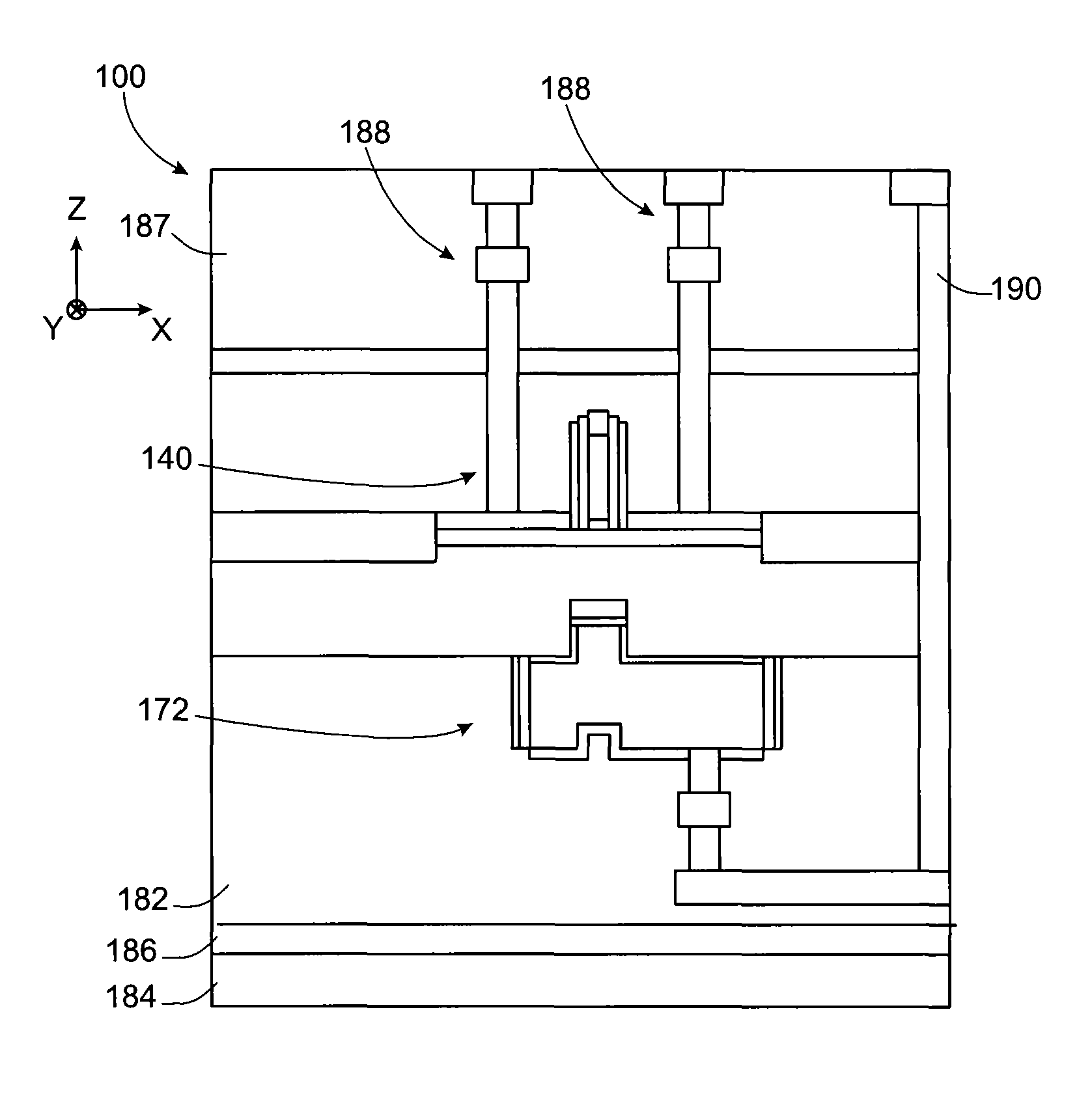
[0084]Reference is made first of all to FIGS. 1 to 14B which show the steps of a method of producing an integrated circuit 100 according to a Although the production of only two MOS devices 140 and 172, here transistors, distributed over two different levels of the integrated circuit 100, are shown in these figures, the method used makes it possible to produce an integrated circuit 100 comprising a plurality of first MOS devices and a plurality of second MOS devices distributed over two different levels of the integrated circuit 100.
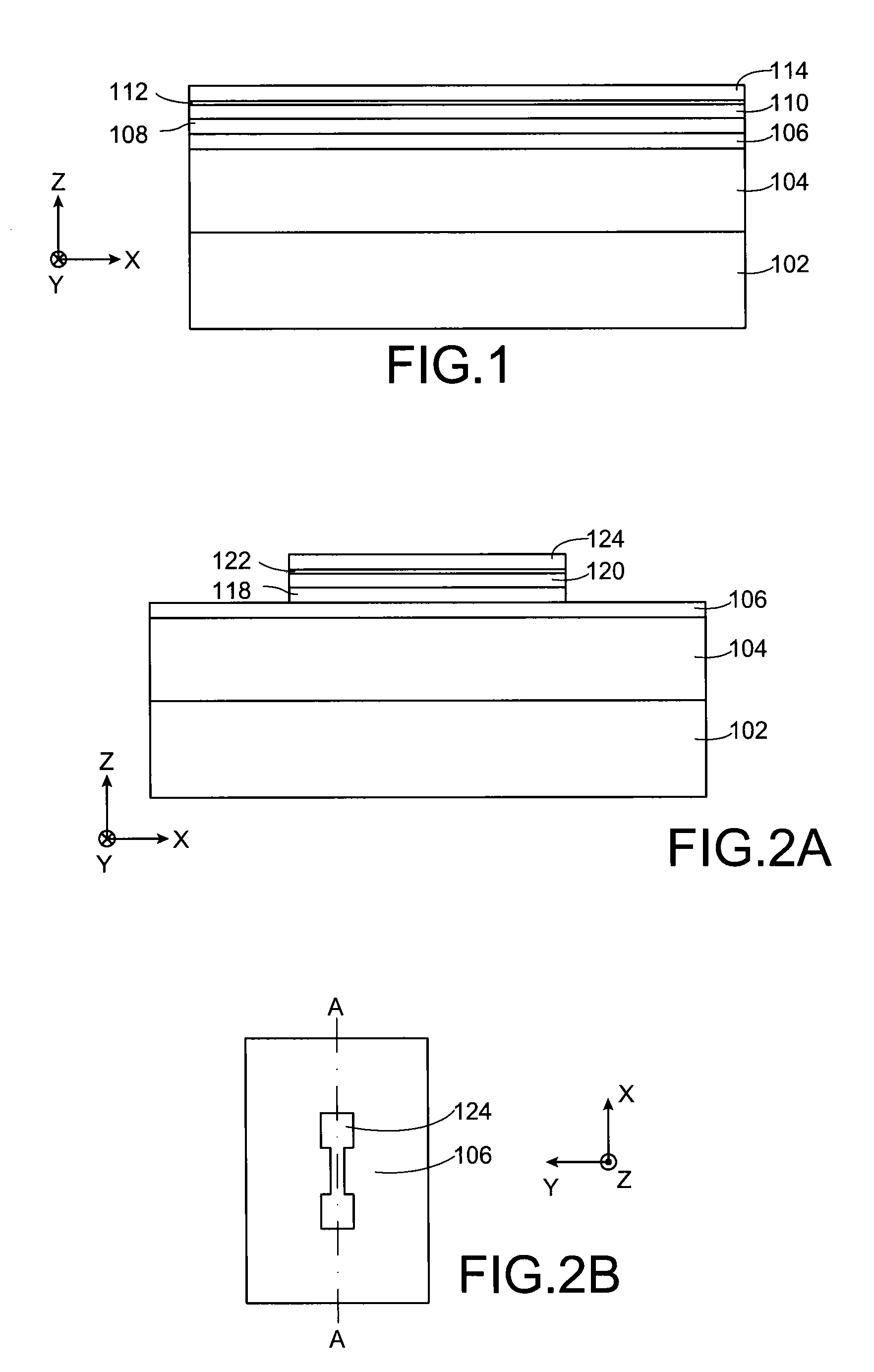
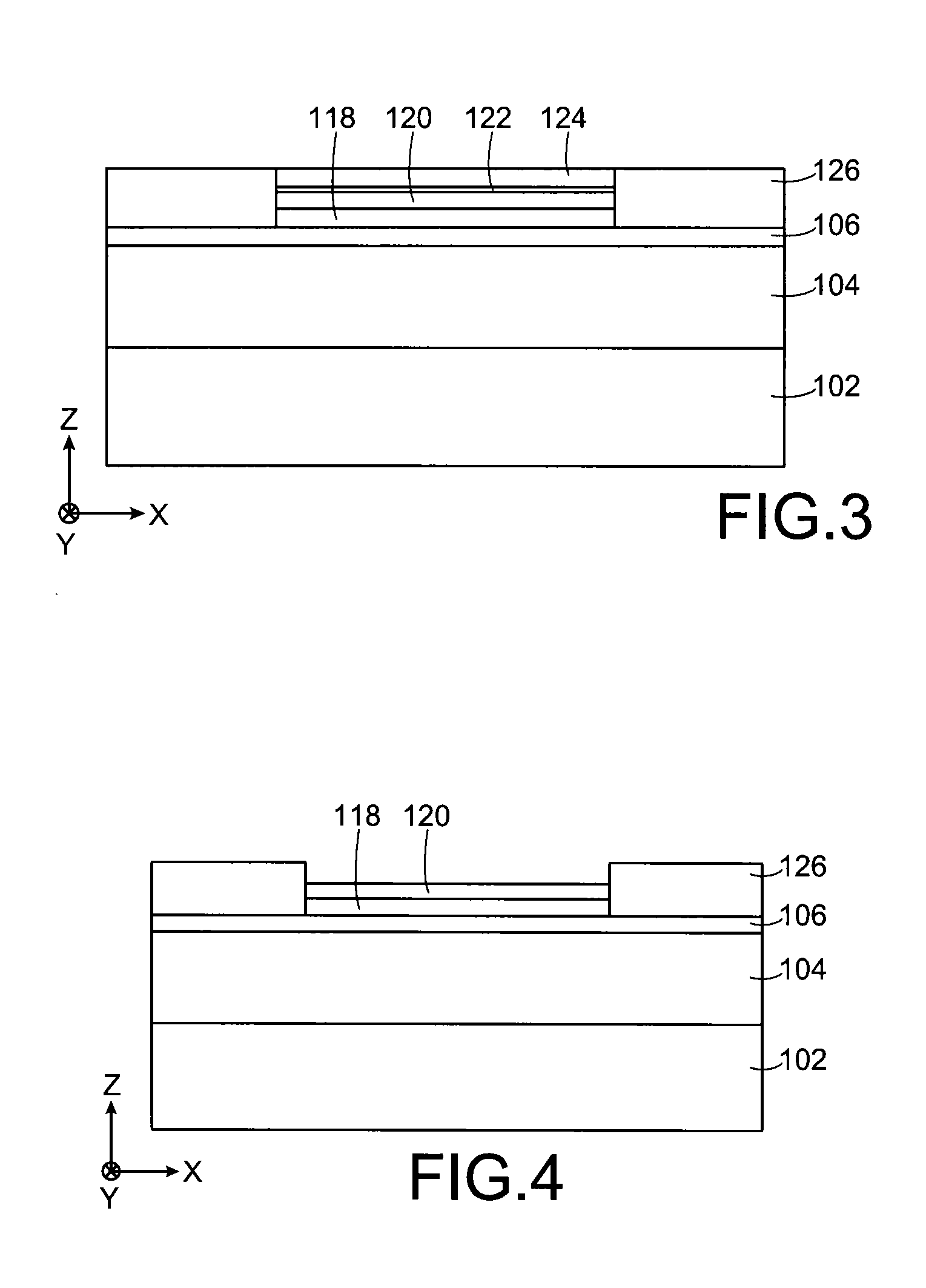
[0085]As shown in FIG. 1, the method is implemented using a substrate of the semiconductor on insulator type, for example SOI, comprising a semiconductor support layer 102, for example composed of silicon, on which a buried dielectric layer 104 is placed, for example composed of SiO2, and a surface layer of semiconductor 106, for example a thin layer of silicon with a thickness less than approximately 10 μm, and preferably less than approximately 100 nm...
third embodiment
[0131]The production of a three-dimensional integrated circuit 300 is now described in relation to FIGS. 16A to 16D.
[0132]The steps previously described in relation to FIGS. 1 to 4 are first performed, forming the future active areas of the first MOS transistors delimited by the dielectric portions 126.
[0133]The future active areas of the first transistors of the NMOS type are then masked by effecting a deposition of nitride 302, a photolithography and an etching of the nitride 302 (FIG. 16A). An epitaxy of SiGe 304 is then effected on the non-masked portions of silicon 120, which therefore correspond to the future active areas of the first PMOS transistors (see FIG. 16B).
[0134]The integrated circuit 300 is computed in a similar manner to the first embodiment. As shown in FIG. 16C, the integrated circuit 300 obtained comprises first MOS transistors, and in particular first NMOS transistors 140a the active areas of which are composed of the semiconductor of the portions 120 and firs...
fourth embodiment
[0138]The production of a three-dimensional integrated circuit 400 is now described in relation to FIGS. 17A to 17E.
[0139]The steps previously described in relation to FIGS. 1 to 9G are first of all performed, forming the first MOS transistors and the future active areas of the second MOS transistors. In this fourth embodiment, at least some of the first and second MOS transistors are replaced by memory cells of the flash type. For this purpose, the second MOS transistors that it is wished to keep as transistors (as well as the first MOS transistors placed opposite the second transistors) are optionally covered with a mask 402 (FIG. 17A).
[0140]As shown in FIG. 17B, the portions 118 of SiGe are next etched at the MOS devices intended to form memory cells. A first layer of oxide 404 is deposited in a conforming manner on the assembly previously produced, covering in particular the portions of silicon 120 forming the active areas of the first MOS devices as well as the stacks of porti...
PUM
 Abstract
Description
Claims
Application Information
 - R&D
- Intellectual Property
- Life Sciences
- Materials
- Tech Scout
- Unparalleled Data Quality
- Higher Quality Content
- 60% Fewer Hallucinations
Browse by: Latest US Patents, China's latest patents, Technical Efficacy Thesaurus, Application Domain, Technology Topic, Popular Technical Reports.
© 2025 PatSnap. All rights reserved.Legal|Privacy policy|Modern Slavery Act Transparency Statement|Sitemap|About US| Contact US: help@patsnap.com