Advanced electrode structures and electrochromic devices

a technology of advanced electrode structure and electrochromic device, applied in the field of electrochromic display device, can solve the problems of common limitations in the design of the working (seg) electrode of electrochromic (and ionochromic) system, and affecting the performance of the display devi

Inactive Publication Date: 2014-07-22
NTERA LTD (IE)
View PDF2 Cites 7 Cited by
  • Summary
  • Abstract
  • Description
  • Claims
  • Application Information

AI Technical Summary

Problems solved by technology

In particular, electronic paper is required to have as excellent white reflectivity and contrast ratio as paper with respect to its display characteristics, and the development of a display device offering all of these characteristics is far from easy.
Regardless of the specific cell architecture, there are common limitations related to the design of the working (SEG) electrode of electrochromic (and ionochromic) systems.
Those limitations come, among matters, from the selection and use of conductors inside the working electrode, namely uniform near transparent conductors, as well as requirements on manufacturing that are not aligned with the most effective manufacturing techniques available for printed electronics.
Transparent conductors tend to break down due to fatigue.
This is a serious limitation for items such a smart labels or credit cards as these items are often bent during use.
This means that PEDOT:PSS has limitations with respect to color performance in electrochromic materials that rely on another material for color changes.
This is a major limitation with respect to optical quality, namely reflectance and contrast ratio.
Most grid-based technologies available are not able to achieve an appropriate performance between conductivity and transparency.
Grid structures are not readily amenable to support a poorly conductive SEG material as lateral conductivity might not be high enough to move charges across wires being printed, and they are not amenable to being printed using screen-printing, a method widely used in printed electronics.
This has two major limitations: 1) it will inherently cause an optical loss and at times the addition of a tint to the working electrode and 2) it is not amenable to patterning.
Optical quality and control of switching are limitations of these designs.
This creates compatibility issues that preclude the selection of specific metal-electrolyte combinations.
This architecture has several limitations.
It has the limitation of not supporting conductive tracks inside the display, managing the coloring of multiple segments inside a single display.
It has the disadvantage of potentially not being scratch-free and can create some parallax issues with the rest of the displays.
It has the disadvantage to not be as roll-to-roll manufacturing friendly and is subject to manufacturing and usage scratches.
This design has limitations with respect to the formulation of the dielectric separator, most notably because it requires additional processing to avoid separation and lumping between pigments, contributing to shorter shelf life for the ink.
These two designs have the same limitations as other legacy designs with respect to selection of materials for the working electrode, separator or electrolytes.
It is also not patterned and cannot be used for color matching.
This limitation results in the need for precise alignment / registration of the printing of chromic layer material.
Based on these capabilities, printing the maximum precision chromic layer is problematic for a roll-to-roll process, especially if the chromic layer is deposited on a conductor layer that has varying thickness or variation in surface energy.

Method used


Image

  • Advanced electrode structures and electrochromic devices
  • Advanced electrode structures and electrochromic devices
  • Advanced electrode structures and electrochromic devices

Examples


Embodiment Construction

[0074]Reference will now be made in detail to the preferred embodiments of the present disclosure, examples of which are illustrated in the accompanying drawings. Wherever possible, the same reference numbers will be used throughout the drawings to refer to the same or like parts.

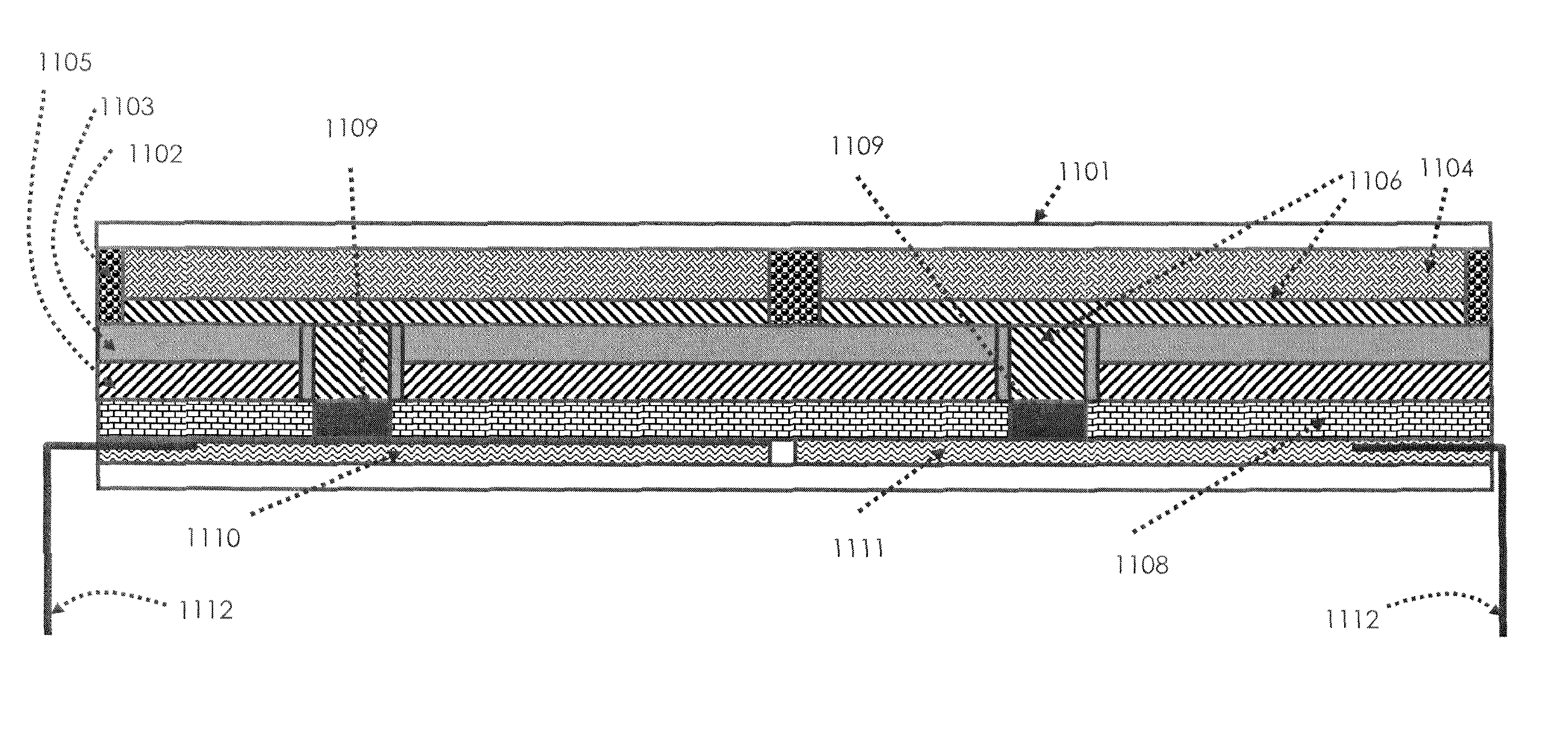
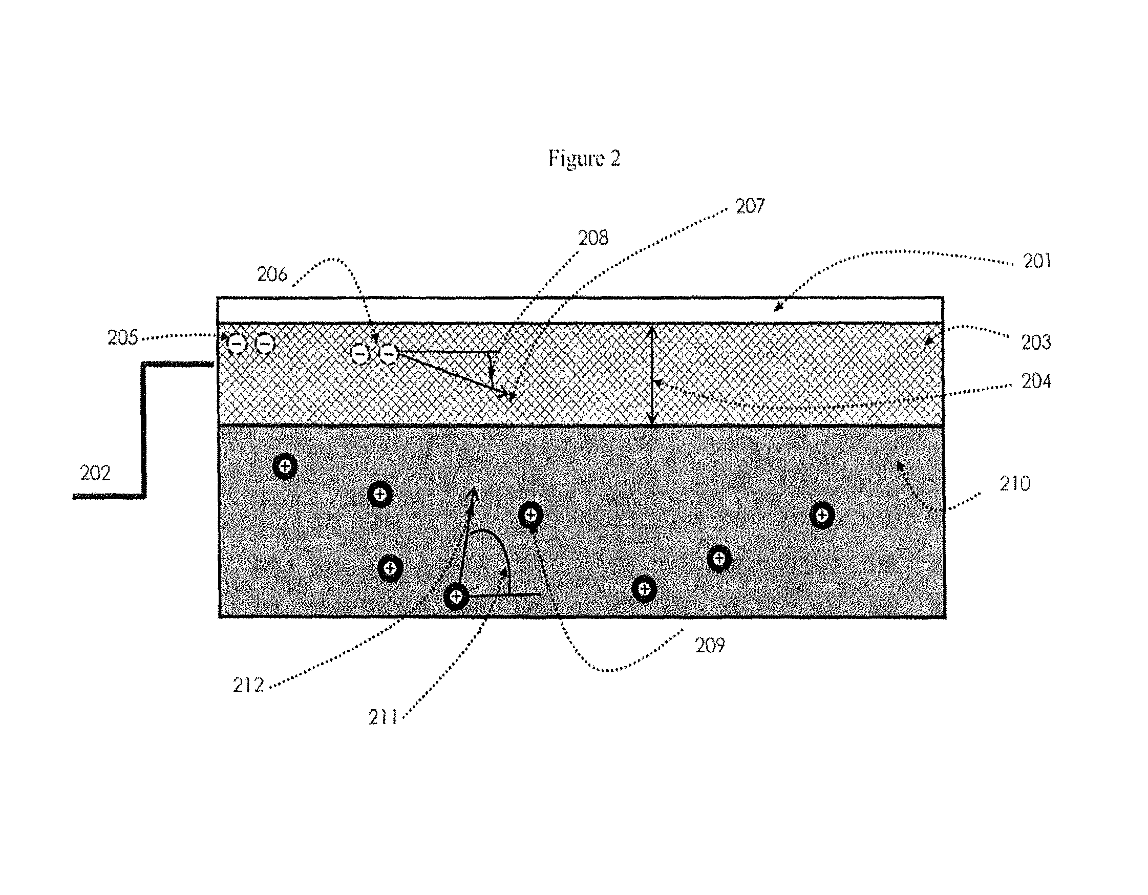
[0075]The present disclosure provides for an inventive display device having: a coloring electrode positioned on a transparent film; a second electrode; a separator layer positioned between the coloring electrode and the second electrode; and electrolyte. The coloring electrode is formed from a connected conductor system of one or more heterogeneous conductive areas and a coloring area where the coloring area is directly deposited onto the transparent film without the heterogeneous conductive areas positioned between the transparent film and the coloring area. The disclosure is summarized in the following sections: (A) Display Design and Method of Manufacture; (B) Material Compositions (used to generate the...


PUM

PropertyMeasurementUnit
reduction potentialaaaaaaaaaa
angleaaaaaaaaaa
temperatureaaaaaaaaaa

Abstract

The present invention provides for a display device and a method to manufacture the display device. The display device includes: a transparent layer; a coloring electrode; a separator; a second electrode; an electrolyte permeating throughout the display device; and a back layer positioned on the back side of the display. The transparent layer, which has a top surface and a bottom surface, is positioned at the viewer side of the display. The coloring electrode is positioned on the transparent layer bottom surface and includes: a connected conductor system formed from one or more heterogeneous conductive layers and a coloring layer, with the proviso that the heterogeneous conductive layers are not positioned between the transparent layer bottom surface and the coloring layer. The conductor heterogeneity includes variations in one or more of: conductor material composition; conductor layer dimension; conductor layer pattern; conductor layer grid design, and combinations thereof. The separator layer is positioned between the coloring electrode and the second electrode.

Description

CROSS REFERENCE TO RELATED APPLICATION[0001]This application is a U.S. National Stage of and claims priority benefit from International Patent Application No. PCT / US2010 / 025149, filed 24 Feb. 2010, now published as WO 2010 / 099147A1, which in turn claims priority benefit from U.S. Provisional Patent Application No. 61 / 155,014, filed 24 Feb. 2009, and U.S. Provisional Patent Application No. 61 / 209,052, filed 3 Mar. 2009, all of which are incorporated herein by reference in their entirety.FIELD OF THE INVENTION[0002]The present invention relates to electrochromic display devices, a method of manufacturing such devices and applications of the devices.BACKGROUND OF THE INVENTION[0003]Much research effort has been made into producing electronic paper as an electronic medium. Electronic paper requires the following characteristics: being reflective rather than emissive; high white (or off white) reflectivity and contrast ratio; allowing high definition images; memory effect (referred to at...

Claims


Application Information

Patent Timeline
Patent Type & Authority Patents(United States)
IPC IPC(8): G02F1/155G02F1/15G09G3/38G02F1/1516G02F1/1523
CPCG02F1/1523G02F1/155G02F1/1525G02F1/15G09G3/38C09K9/02C09K2211/1007C09K2211/1029G02F1/1533G02F1/157G02F1/1516
Inventor COPELAND, GAVINBRIANCON, ALAINMOELLER, MARTINLEYLAND, NIGELGIACOPONELLO, CHRISCASSIDY, MICHEALGRAVE, CHRISTIANCORR, DAVIDBEVK, DAVIDRYAN, MICHAEL
Owner NTERA LTD (IE)
Why Eureka
Try Eureka