Liquid crystal display device, black matrix substrate and color filter substrate
a liquid crystal display device and black matrix technology, applied in the field of liquid crystal display devices, can solve the problems of increasing the thickness of the liquid crystal display device, and affecting the operation of the touch panel
- Summary
- Abstract
- Description
- Claims
- Application Information
AI Technical Summary
Benefits of technology
Problems solved by technology
Method used
Image
Examples
first embodiment
(First Embodiment)
[0049]In the present embodiment, a liquid crystal display device will be described which is capable of receiving optical signals and which suppresses the adverse effect of an external light condition on display quality, the liquid crystal display device reducing malfunction.
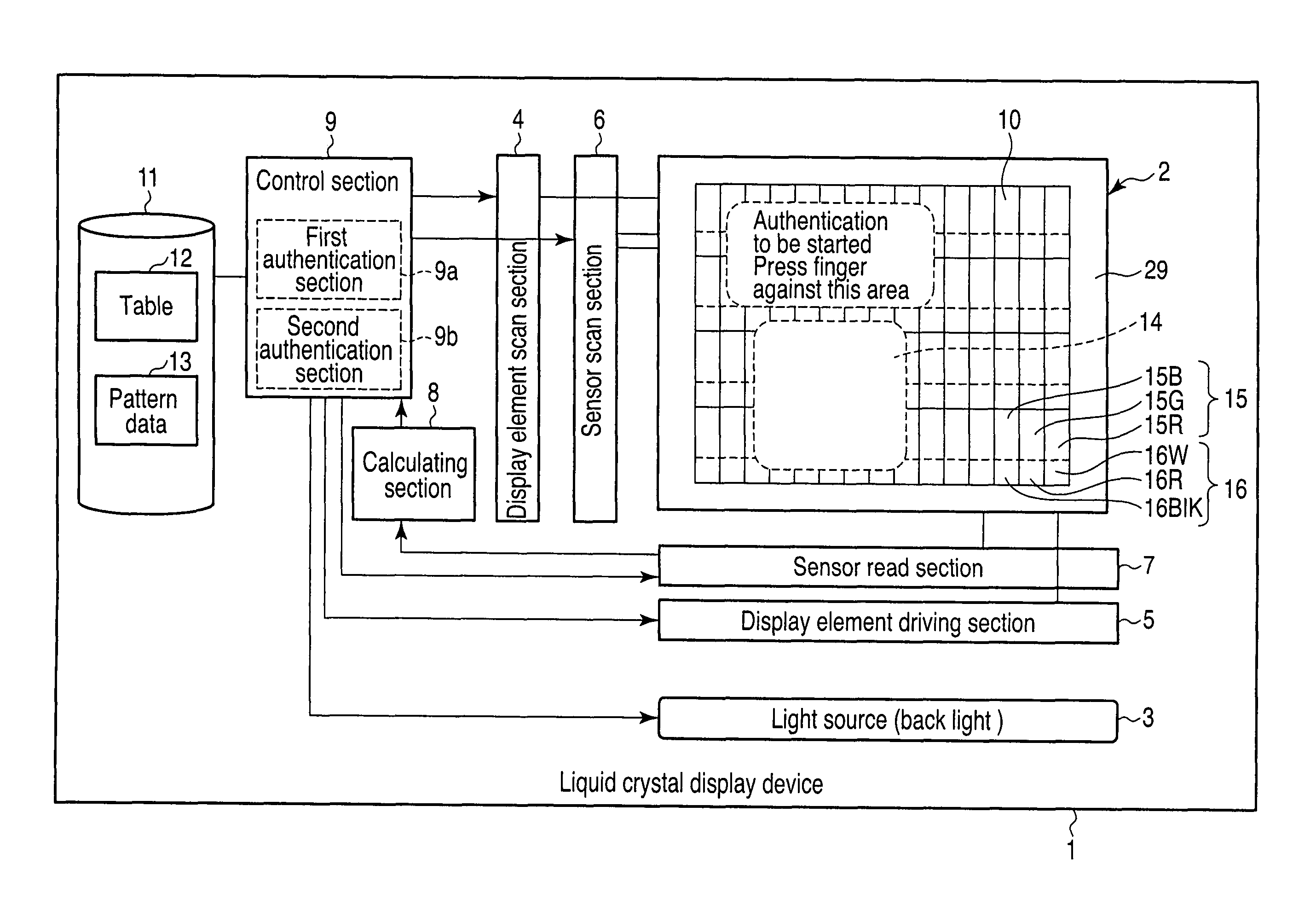
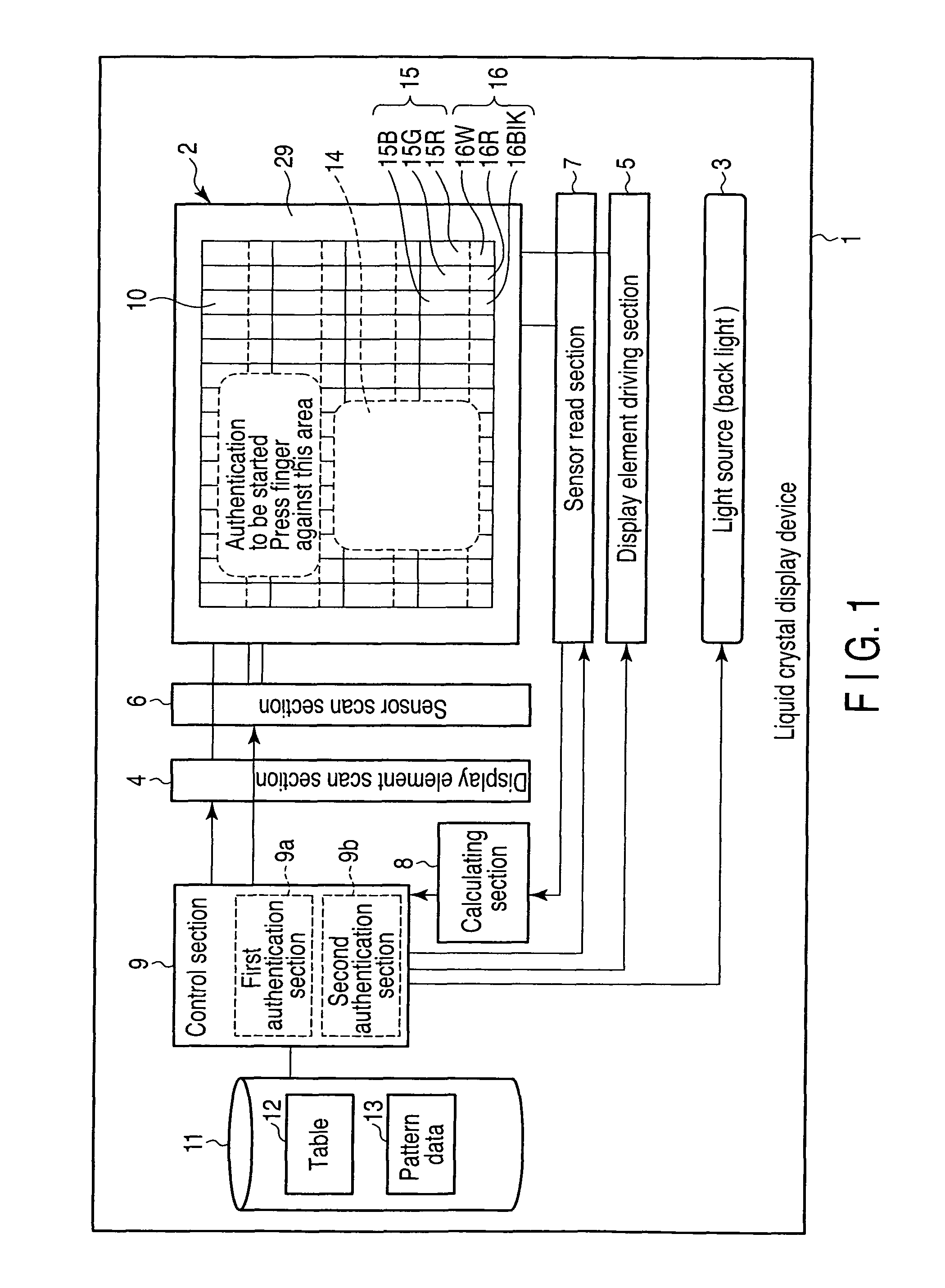
[0050]FIG. 1 is a block diagram showing an example of the liquid crystal display device according to the present embodiment.
[0051]The liquid crystal display device 1 according to the present embodiment comprises a light source 3 in the rear of a display screen section 2 (the display screen section 2 is shown at the bottom of FIG. 1 for easy understanding). The light source 3 emits light with three wavelengths for blue, green, and red. For example, the light source 3 may be a fluorescent lamp or LED elements of three-wavelength light emission type, or organic EL elements of a surface light emission type.
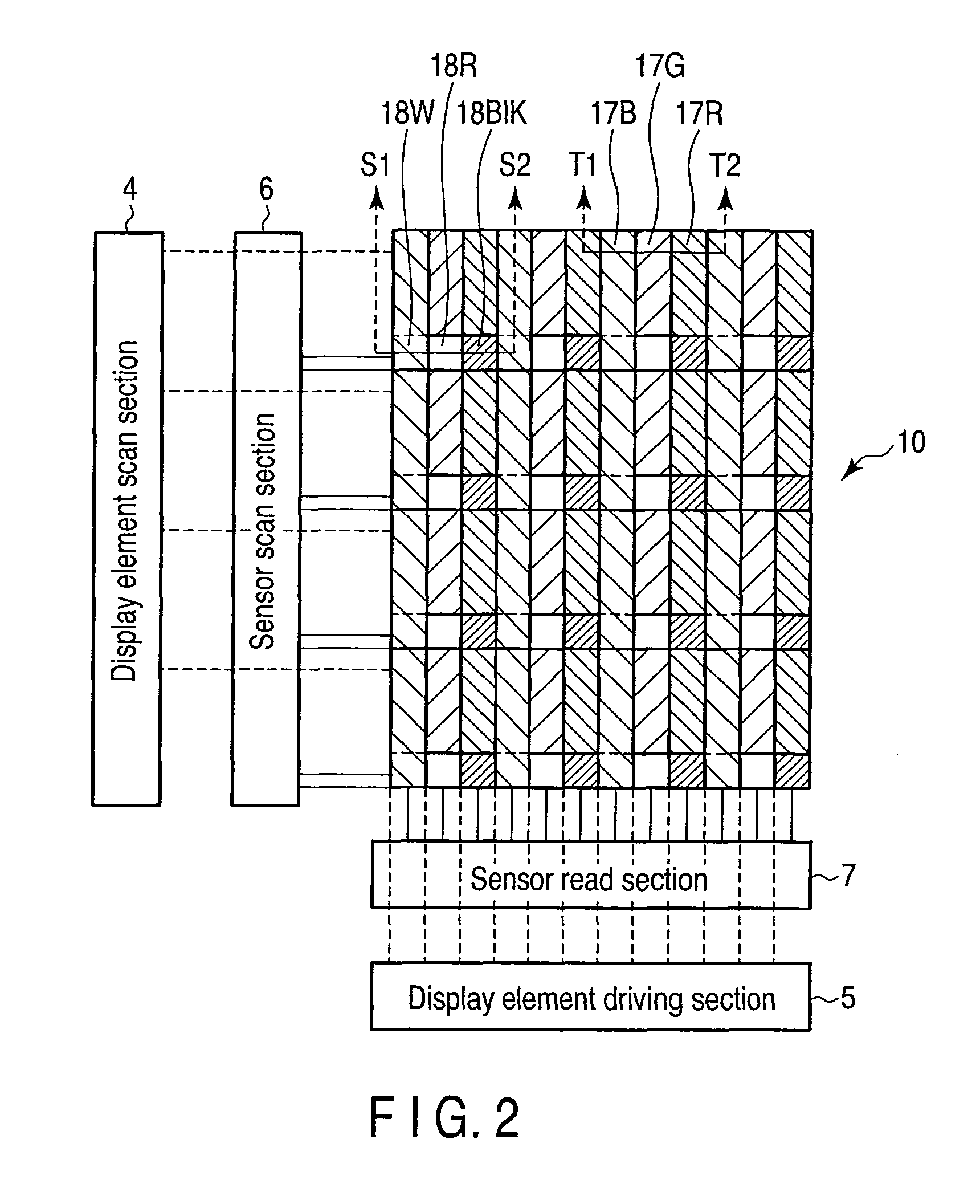
[0052]A display element scan section 4, a display element driving section 5, a sensor scan sec...
second embodiment
(Second Embodiment)
[0167]In the present embodiment, a modification of the above-described first embodiment in which an infrared transmission filter is formed of a stack of a plurality of filters will be described.
[0168]FIG. 13 is a sectional view showing an example of a light detection pixel provided in a liquid crystal display device according to the present embodiment.
[0169]In the present embodiment, an infrared transmission filter 30Blk is formed of a stack of a red filter 31 and a blue filter 32.
[0170]In the present embodiment, a plurality of openings 33 through which light enters the pixel are formed in a substrate 25. The openings 33 are located opposite the infrared transmission filter 30Blk, a red filter 18R, and a short-wavelength transmission filter 18W via a liquid crystal 22, respectively. Optical sensors 20Blk, 20R, and 20W each receive light to be observed, via the plurality of openings 33, a liquid crystal 22, and a corresponding one of the infrared transmission filte...
third embodiment
(Third Embodiment)
[0172]In the present embodiment, description will be given of a modification of the first and second embodiments in which a liquid crystal display device comprises a light detection pixel 16 further including a yellow pixel.
[0173]FIG. 14 is a block diagram showing an example of a liquid crystal display device according to the present embodiment.
[0174]A liquid crystal display device 30 according to the present embodiment comprises a light source 3 behind a display screen section 31. A display element scan section 4, a display element driving section 5, a sensor scan section 6, and a sensor read section 7 are electrically connected to the display screen section 31.
[0175]The display screen section 31 comprises a color filter 32. In the present embodiment, display pixels 33 and light detection pixels 34 are disposed in the display area of the display screen section 31. The light detection pixels 34 are arranged on the display screen at almost equal intervals.
[0176]The ...
PUM
| Property | Measurement | Unit |
|---|---|---|
| transmittance | aaaaa | aaaaa |
| optical wavelength | aaaaa | aaaaa |
| wavelength | aaaaa | aaaaa |
Abstract
Description
Claims
Application Information
 - R&D
- Intellectual Property
- Life Sciences
- Materials
- Tech Scout
- Unparalleled Data Quality
- Higher Quality Content
- 60% Fewer Hallucinations
Browse by: Latest US Patents, China's latest patents, Technical Efficacy Thesaurus, Application Domain, Technology Topic, Popular Technical Reports.
© 2025 PatSnap. All rights reserved.Legal|Privacy policy|Modern Slavery Act Transparency Statement|Sitemap|About US| Contact US: help@patsnap.com


