
Dielectric materials, methods of forming subassemblies therefrom, and the subassemblies formed therewith

a dielectric material and dielectric technology, applied in the field of polymeric dielectric materials, methods of forming circuit subassemblies and circuits, can solve the problems of affecting the electrical properties of the subassembly, the loss of conventional dielectric materials at the higher frequency (e.g., gigahertz) frequency, and the level of many high frequency/high speed applications can be problemati

Active Publication Date: 2014-01-21
ROGERS CORP
View PDF42 Cites 8 Cited by
  • Summary
  • Abstract
  • Description
  • Claims
  • Application Information

AI Technical Summary

Benefits of technology

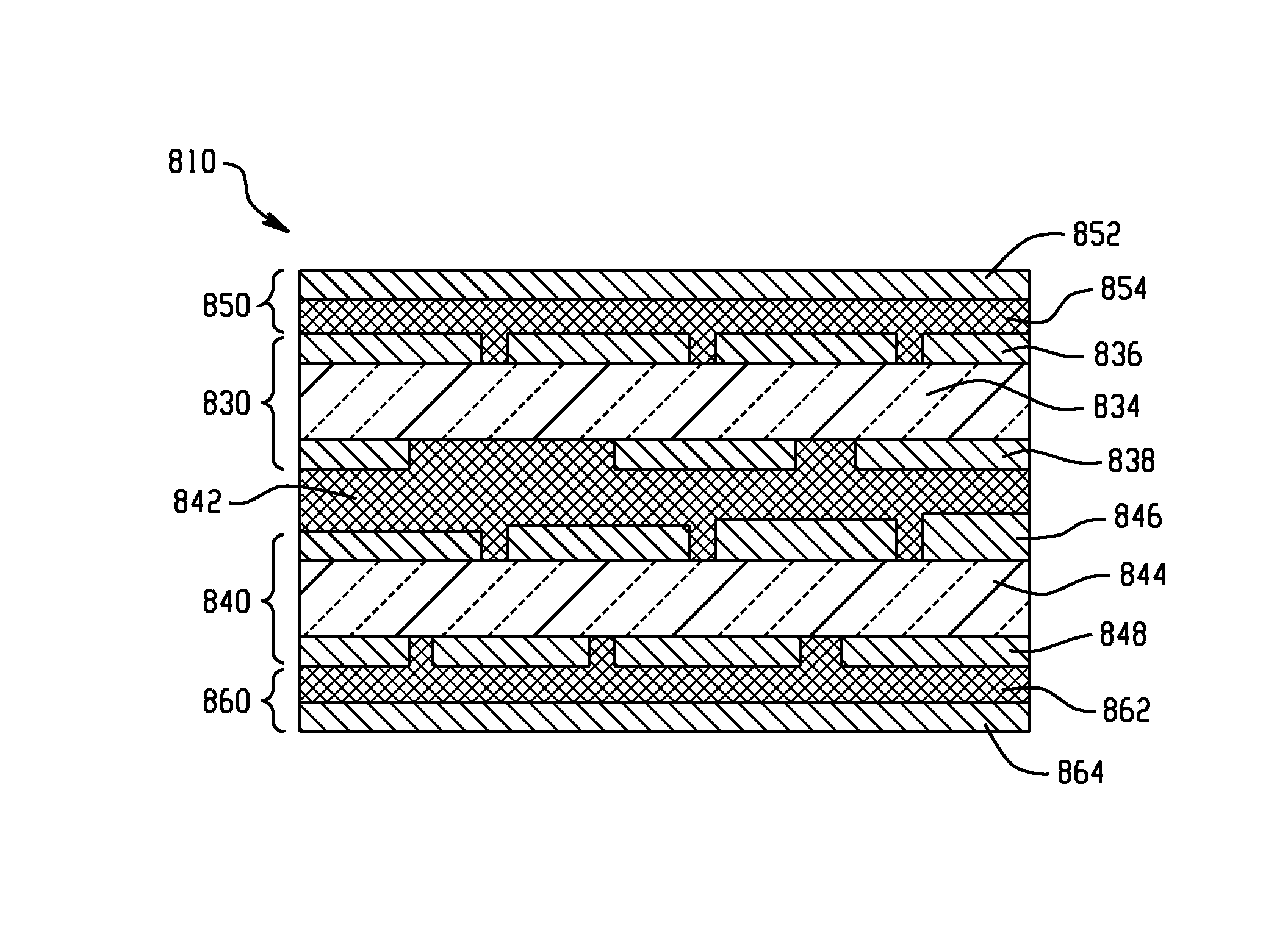
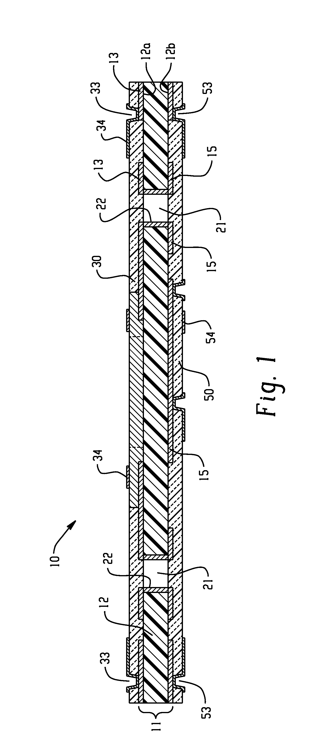
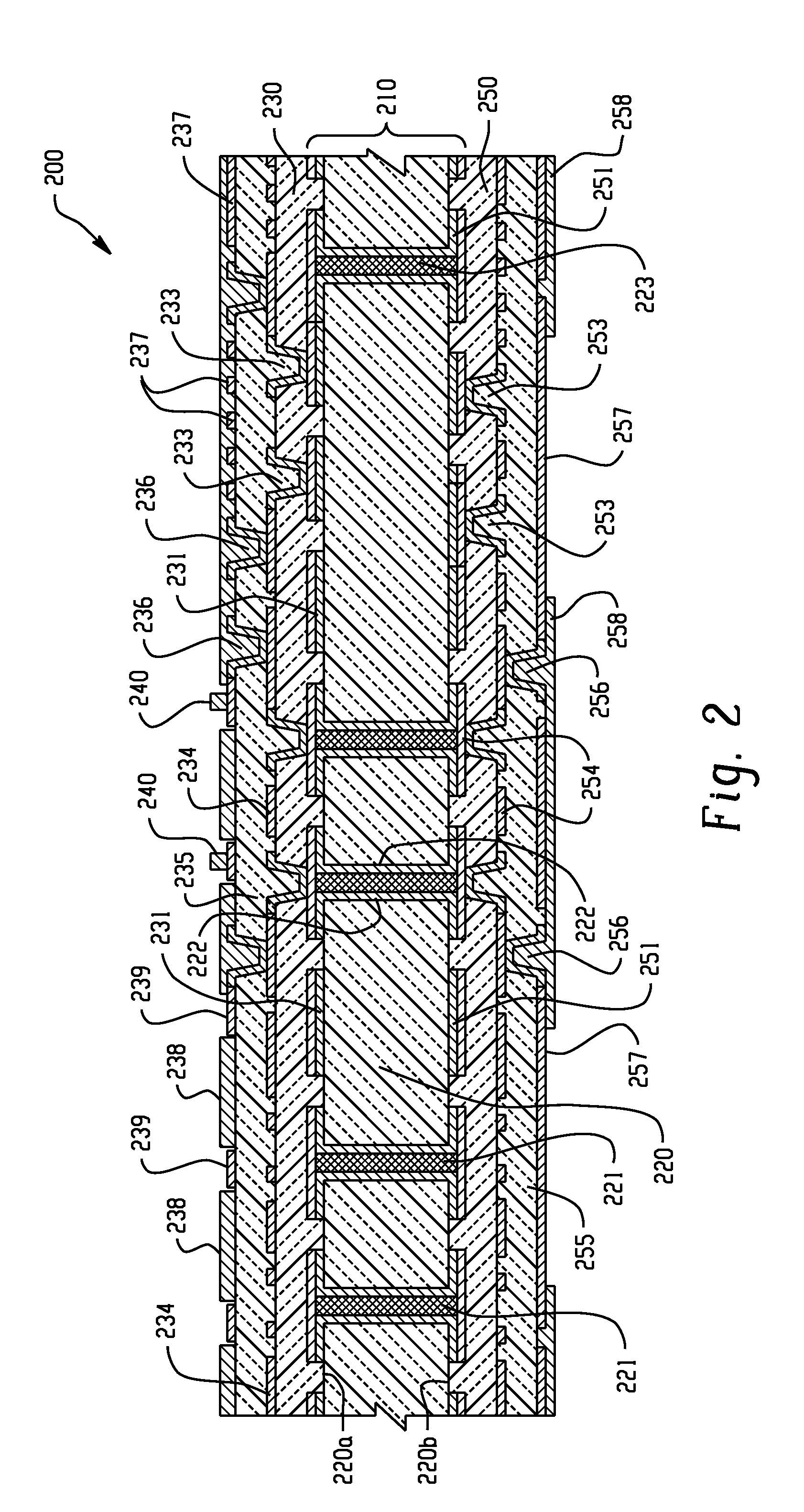
This patent describes a dielectric composition that can be used in various circuit subassemblies and multilayer circuits. The composition includes a dielectric filler and a thermosetting composition made up of a poly(arylene ether) and a carboxy-functionalized polymer. The composition can be used as a buildup layer, a core adhesive layer, a resin-coated conductive layer, a dielectric layer, and more. The patent also describes a sequential buildup subassembly comprising a core and a dielectric buildup layer, as well as methods for manufacturing the circuit subassembly and multilayer circuit. The technical effect of the invention includes improved performance and reliability of circuit components.

Problems solved by technology

However, conventional dielectric materials can have relatively high loss at the higher (e.g., gigahertz) frequencies.
For example, a commonly used buildup dielectric film, type GX13 from Ajinomoto, has a loss of 0.019 at 5.8 GHz (Ajinomoto data sheet on ABF materials dated June 2007), which level can be problematic for many high frequency / high speed applications.
In addition, absorbed water in the buildup dielectric can have adverse effects on electrical properties, especially in increasing loss, and thereby creating electrical reliability problems.
The aforementioned GX13 buildup dielectric film has a water absorption of greater than 1% which is unacceptable for many high frequency / high speed applications.
Such high water absorption also can lead to thermal reliability problems.
Further, the capacitance density of conventional dielectric materials can change as a function of frequency and temperature, which can affect the performance of the package.
Dielectric materials in present use, such as the afore-mentioned GX13, have many of the desired properties sought for buildup applications, but do not meet all the desired needs for increasing high frequency / high speed applications.
These materials suffer especially from having dielectric loss and water absorption considerably higher than desired and high temperature thermal performance less than desired.

Method used


Image

  • Dielectric materials, methods of forming subassemblies therefrom, and the subassemblies formed therewith
  • Dielectric materials, methods of forming subassemblies therefrom, and the subassemblies formed therewith
  • Dielectric materials, methods of forming subassemblies therefrom, and the subassemblies formed therewith

Examples


examples

[0114]The materials in Table 1 were used in the following examples.

[0115]

TABLE 1Material Name ™Chemical NameSupplierBlendex HPP820Unmodified polyphenylene etherChemtura(PPE)Noryl 640-111Unmodified polyphenylene etherSabic Innovative(PPE)PlasticsSA5587Methacrylic Anhydride CappedSabic InnovativePPEPlastricsOPE-2STYStyrenated polyphenylene etherMitsubishi GasCompanyKraton D-1118SB diblock copolymer (20%)Kraton Polymersand SBS triblock copolymer(80%)Ricon 184 MA-6Maleinated butadiene-styreneSartomercopolymerTAICTrially isocyanurateAldrichPerkadox 30 / Curing agentAkzo NobelVaroxSC 2050 TNGSilica dispersion in tolueneAdmafine (Japan)BA-188Silica powderCE MineralsKisuma 8SNMagnesium hydroxideKyowa ChemicalsCAB-O-SILFumed silica powderCabot CorporationTS-720Budit 3141CAMelamine polyphosphateBudenheimTiPure 101Titanium dioxide powderDuPontAngular BNTBarium nanotitanateDimat IncCode 218Strontium titanateFerro Corp.ChimassorbAntioxidantCIBA944LD

[0116]Minimum melt viscosity was measured using t...


PUM

PropertyMeasurementUnit
thicknessaaaaaaaaaa
volume percentaaaaaaaaaa
weight percentaaaaaaaaaa

Abstract

A circuit subassembly, comprising a dielectric layer formed from a dielectric composition comprising, based on the total volume of the composition: about 15 to about 65 volume percent of a dielectric filler; and about 35 to about 85 volume percent of a thermosetting composition comprising: a poly(arylene ether), and a carboxy-functionalized polybutadiene or polyisoprene polymer.

Description

CROSS REFERENCE TO RELATED APPLICATION[0001]This application claims the benefit of U.S. Provisional Application No. 61 / 186,221 filed on Jun. 11, 2009, which is a continuation-in-part of U.S. application Ser. No. 11 / 829,406 filed on Jul. 27, 2007, which claims the benefit of U.S. Provisional Application No. 60 / 821,710 filed Aug. 8, 2006, all of which are incorporated herein by reference in their entirety.BACKGROUND[0002]This invention generally relates to polymeric dielectric materials, methods of forming circuit subassemblies and circuits that include the polymeric dielectric materials, and the subassemblies and circuits formed thereby.[0003]Polymeric dielectric materials are in wide use in the manufacture of electronic circuits. The polymeric dielectric materials are often supplied to the circuit or device manufacturer as a layer in the form of a circuit subassembly. Such subassemblies are used in many semiconductor packaging applications, such as integrated circuit (IC) substrates...

Claims


Application Information

Patent Timeline
Patent Type & Authority Patents(United States)
IPC IPC(8): B32B25/02H01L49/00B32B25/08H10N99/00
CPCC08L13/00H05K3/4626H05K2201/0355H05K2201/10378H05K2201/0133C08G65/485H05K3/4676B32B15/14C09J171/12C08L9/00H05K1/0393C08K3/0033C08L19/006C08L71/12H05K3/462C08L71/126H05K3/4641C08L15/00C09J107/00C09J113/00H05K2201/0158B32B7/12C08L51/04Y10T428/31544Y10T428/31931H05K3/00Y10T156/10Y10T428/24802Y10T428/263B32B5/08B32B5/16B32B5/30B32B15/06B32B15/08B32B15/16B32B15/20B32B25/08B32B25/14B32B27/08B32B27/12B32B27/14B32B27/20B32B27/26B32B27/285B32B27/302B32B27/32B32B27/38B32B3/04B32B3/08B32B3/18B32B3/30B32B2255/10B32B2255/205B32B2260/025B32B2260/046B32B2262/0269B32B2262/101B32B2262/14B32B2264/10B32B2264/102B32B2264/104B32B2264/12B32B2270/00B32B2307/202B32B2307/204B32B2307/30B32B2307/302B32B2307/3065B32B2307/308B32B2307/7265B32B2457/00B32B2457/08C08L2666/08C08L2666/14C08K3/013C08L2666/04
Inventor PAUL, SANKARKENNEDY, SCOTT D.BAARS, DIRK M.
Owner ROGERS CORP
Learn More