
Socket with integrated damping resistor

a damping resistor and socket technology, applied in the direction of coupling device connection, coupling parts engagement/disengagement, support structure mounting, etc., can solve the problems of complication in board design in the memory module system, and facilitate the downsize and thin circuit board system. , the effect of reducing the damping resistor required

Inactive Publication Date: 2014-01-21
SENSATA TECHNOLOGIES INC
View PDF8 Cites 2 Cited by
  • Summary
  • Abstract
  • Description
  • Claims
  • Application Information

AI Technical Summary

Benefits of technology

This patent improves the design of circuit boards by adding a resistive function to a contact, which reduces the number of damping resistors needed. This makes the circuit board smaller and more compact. It also simplifies the design process.

Problems solved by technology

Consequently, there were problems in facilitating to downsize and thin the memory module system.
Furthermore, as the number of sockets and / or memory modules mounted on the motherboard 20 is increased, more damping resistors are required for the signal lines, which causes the complication of board design in the memory module system.

Method used


Image

  • Socket with integrated damping resistor
  • Socket with integrated damping resistor
  • Socket with integrated damping resistor

Examples


Embodiment Construction

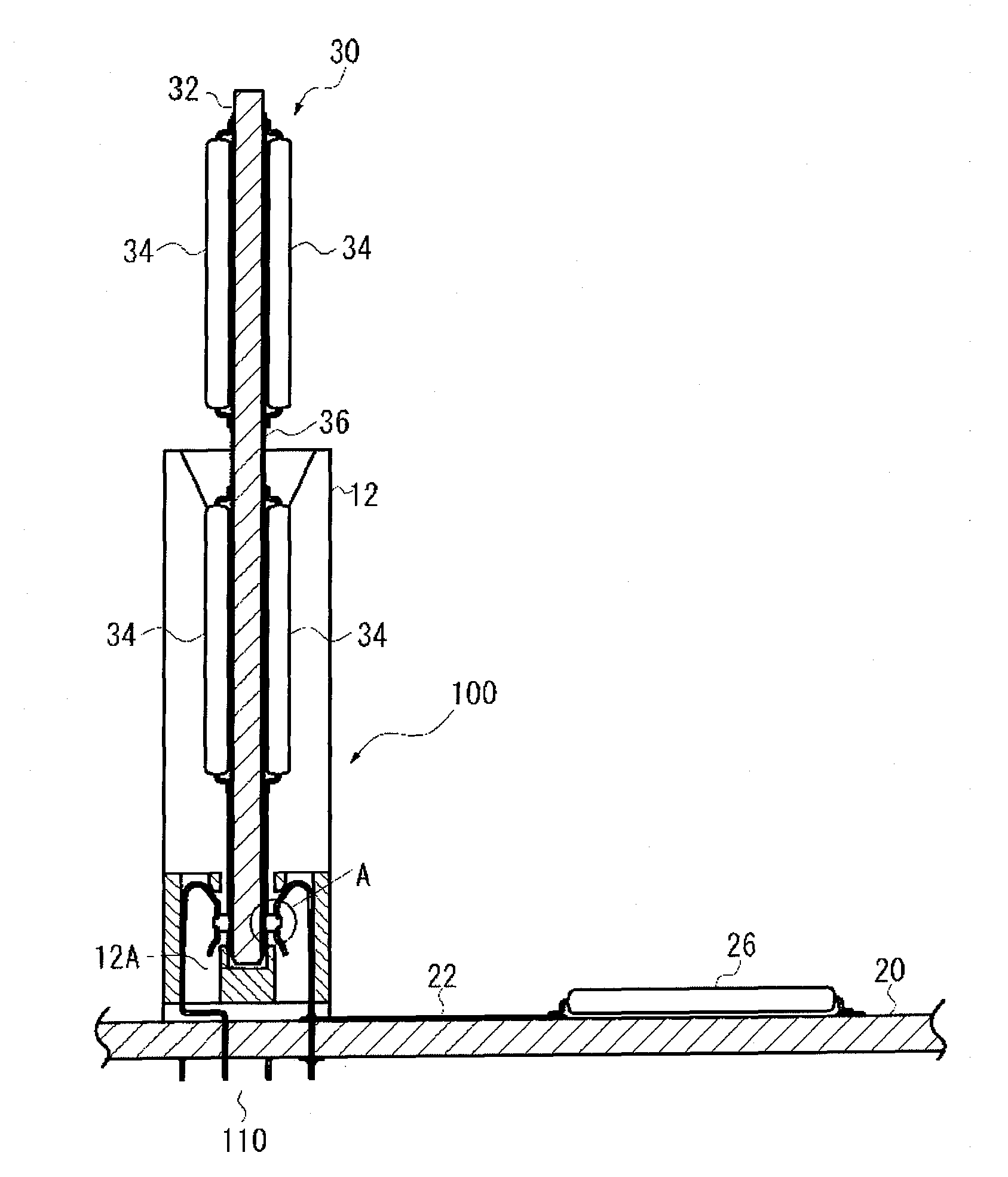
[0031]Disclosed herein is a socket that is installed in a circuit board that requires damping resistors to prevent noise and / or ringing of carried signal on the circuit board. The circuit board may be a module on which is mounted a plurality of semiconductor chips or memory chips, and the semiconductor chips or memory chips are electrically connected through signal lines of conductive traces formed on the surface or inside of the circuit board. A memory module system with a motherboard having a socket with a memory module is described below. It should be noted that the scale in the drawings is represented to understand the present invention easily and it does not express the actual scale of products.

[0032]FIG. 4 shows a configuration of a memory module system in accordance with an embodiment of the present invention. The conventional configurations as described in FIGS. 1A-1D and FIGS. 2A-2D have some elements in common and the same respective reference numbers are used and their ex...


PUM


Abstract

This invention provides a socket for a circuit board that adds function of electrical resistive element to a contact. A socket includes a socket body extending at a longitudinal direction; and a plurality of contacts disposed in two lines along the longitudinal direction of the socket body. When a memory module is connected to the socket body, terminals formed on opposite surfaces of the memory module are electrically and elastically connected by the contacts. The contact includes a contact portion which contacts the terminal, a bent portion for generating an elastic force, and a base portion. The contact is made of a conductive metal having elastic properties, and the contact used for carrying signal is provided with a resistor of an electrical resistive material that is different from the conductive metal. The resistor is connected in a current path between the base portion and the terminal of the memory module.

Description

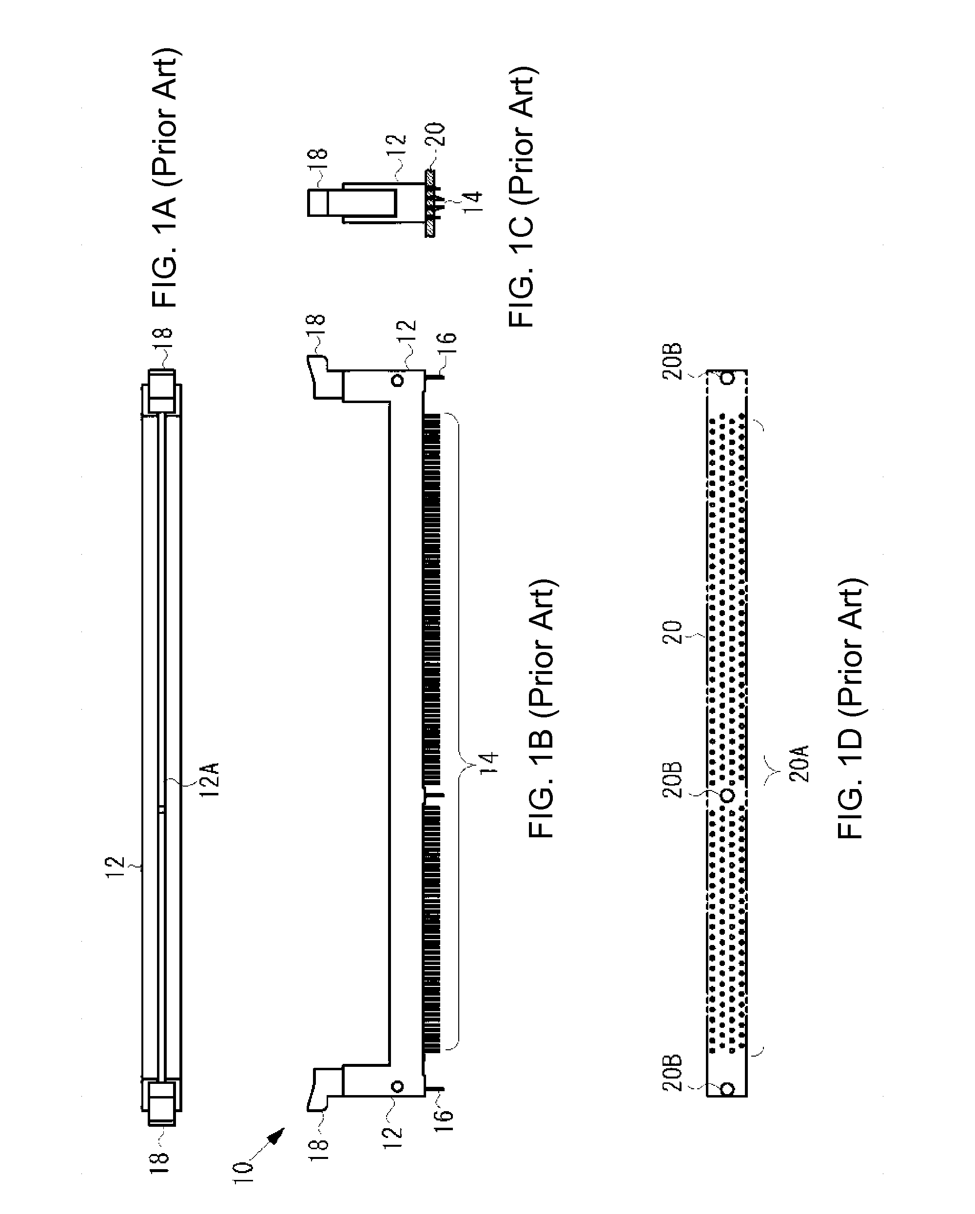
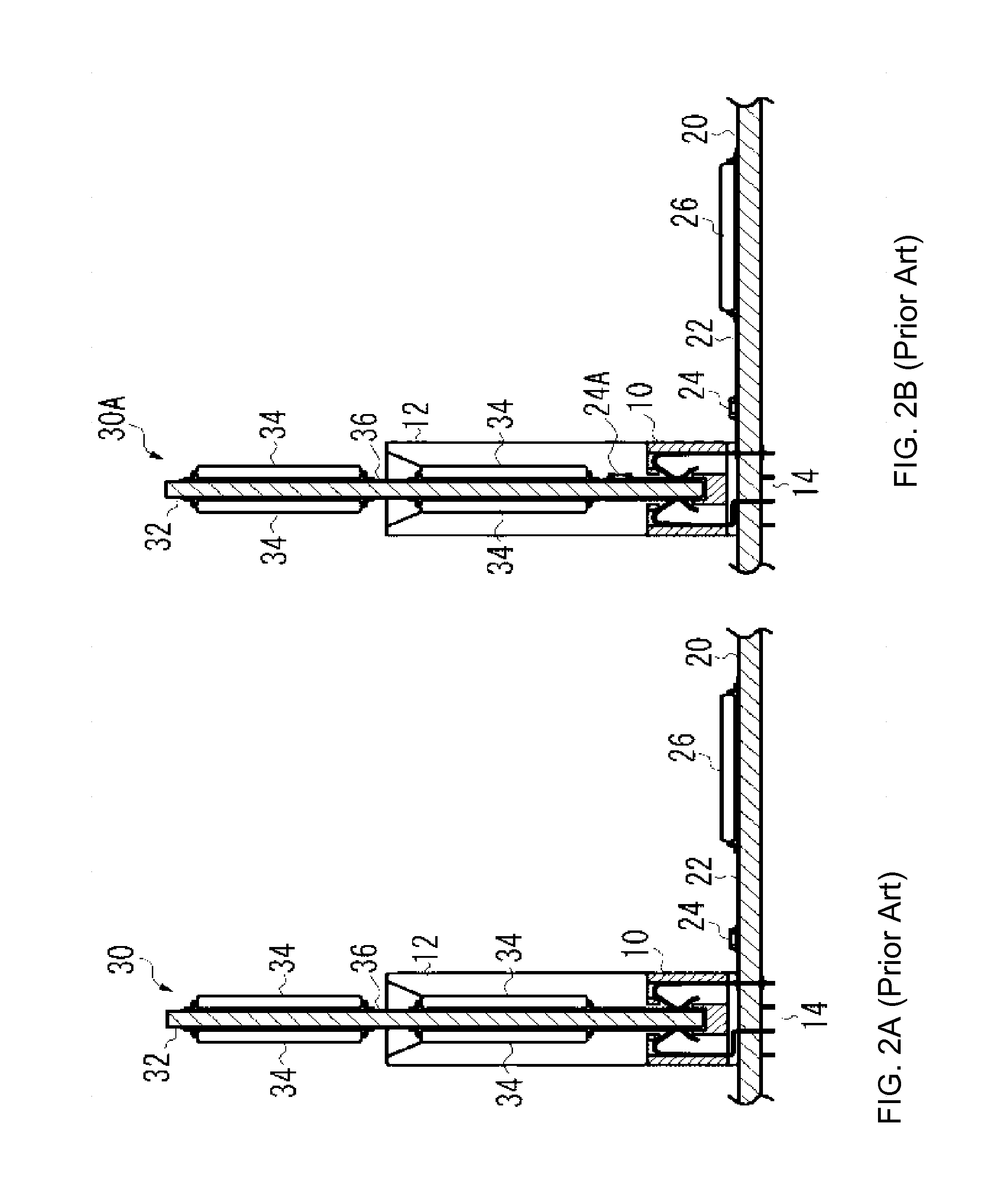
CROSS REFERENCE TO RELATED APPLICATIONS[0001]The present application claims priority to Japanese Patent Application No. 2011-078596, filed 31 Mar. 2011, which is incorporated herein by reference in its entirety.FIELD OF THE INVENTION[0002]The present invention relates to a socket installed on a circuit board, more particularly, to a memory module with a plurality of memory chips installed in a socket and to a memory module system using the socket.RELATED ART[0003]A memory module having mass storage is configured to mount a plurality of semiconductor memory chips, such as dynamic random access memory (DRAM), statistic random access memory or flash memory, at single side of both sides of the circuit board. Such memory module is installed on a socket and the socket is installed on a motherboard to make up a memory module system. Japanese patent publication 2002-298998, 2001-110532 and 2000-173699 discloses a socket installing the memory module.[0004]FIGS. 1A-1C show a conventional sock...

Claims


Application Information

Patent Timeline
Patent Type & Authority Patents(United States)
IPC IPC(8): H01R24/00
CPCH01R12/716H01R13/2442H01R13/6616H01R12/72H01R33/76H05K7/14
Inventor SANO, HIDEKIABEISHIKAWA, YASUSHIEZURA, TOYOKAZUTSUKADA, YASUHISA
Owner SENSATA TECHNOLOGIES INC
Learn More