
Fingerprint sensing device

a technology of fingerprint and sensing device, which is applied in the field of fingerprint sensing device, can solve the problems of electrostatic discharge or esd, the size of the sensor, and the ideal candidate for use on a small sized handheld device which provides only a limited amount of footprin

Active Publication Date: 2013-12-10
AVAGO TECH INT SALES PTE LTD
View PDF12 Cites 46 Cited by
  • Summary
  • Abstract
  • Description
  • Claims
  • Application Information

AI Technical Summary

Benefits of technology

This patent describes a fingerprint sensing device that can be embedded in a touch screen device. It includes a sensor, light source, motion detector and image processor. The device can capture fingerprint images and process them to determine finger movement. This technology provides a secure and comfortable way to verify the identity of electronic devices, providing better security and protection of data.

Problems solved by technology

For such devices, a main challenge is the size of the sensor, since it is more desirable to have a sensor with a small footprint.
However, a disadvantage of such approach is that the die size of the capacitive based sensor must be large enough to provide sufficient contact area for the finger to touch; therefore it is not an ideal candidate for use on a small sized handheld device which provides only a limited allowable foot print.
Another drawback of such a capacitive based sensor is the issue of electrostatic discharge or ESD.
The electrostatic discharge from the human body through the finger can damage the electrode.
Additionally, it can be a challenge in acquiring a good quality image when the dryness or moisture level of the finger surface varies; the degree of moisture on the finger surface can cause the fingerprint recognition system to output erroneous results.
Since such system is based on the capacitive method, most of the above mentioned limitations which are associated with capacitive type sensor devices are unavoidable.
Accordingly, such an approach employs complicated image processing methods and requires high processing power in order to obtain an image quality needed to generate a useful fingerprint image for enabling fingerprint authentication.
However, due to the large size of such module, complexity in its structure and lack of product robustness, such method is not suitable for assembly on a small size portable electronics device.

Method used


Image

  • Fingerprint sensing device
  • Fingerprint sensing device
  • Fingerprint sensing device

Examples


Embodiment Construction

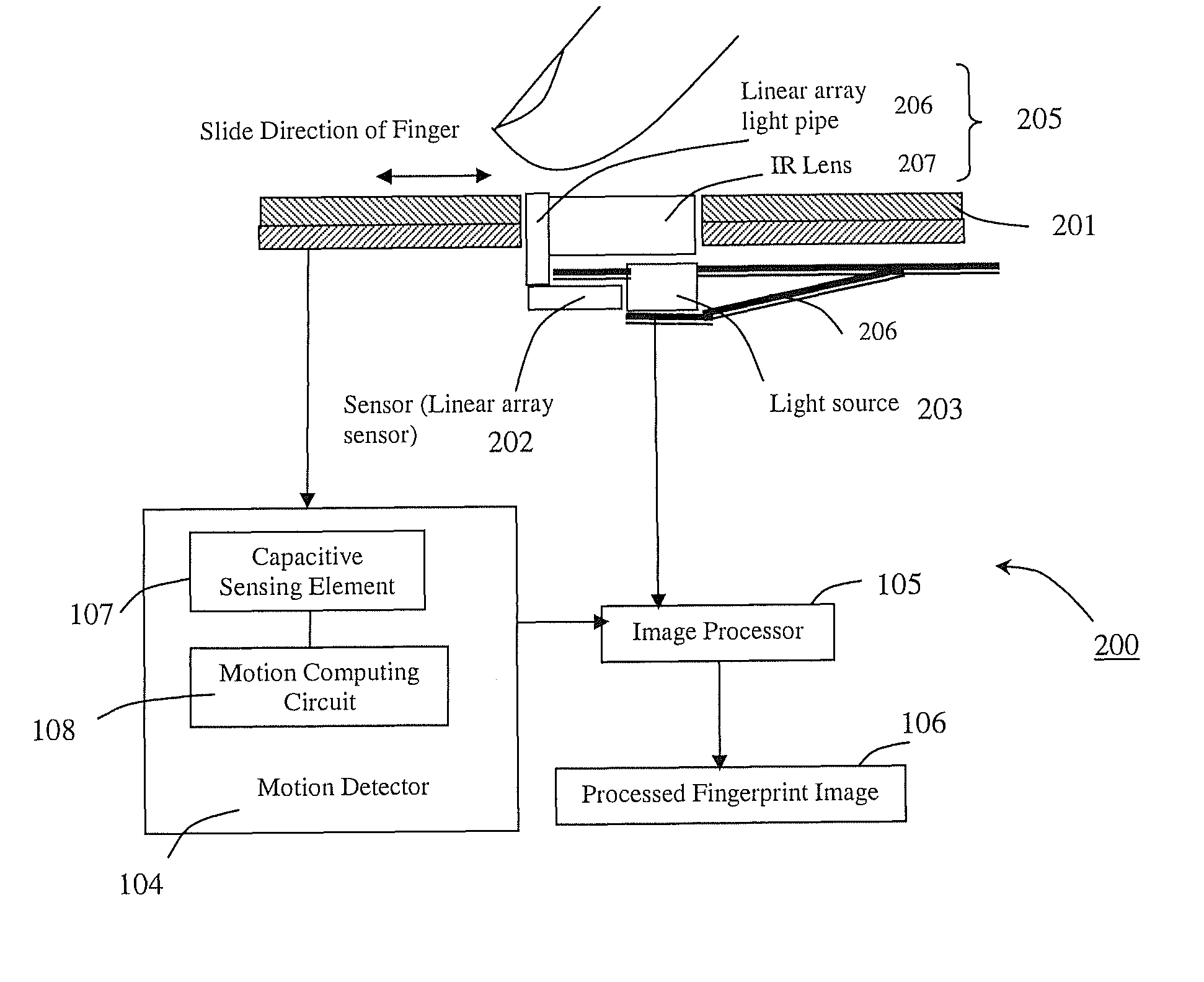
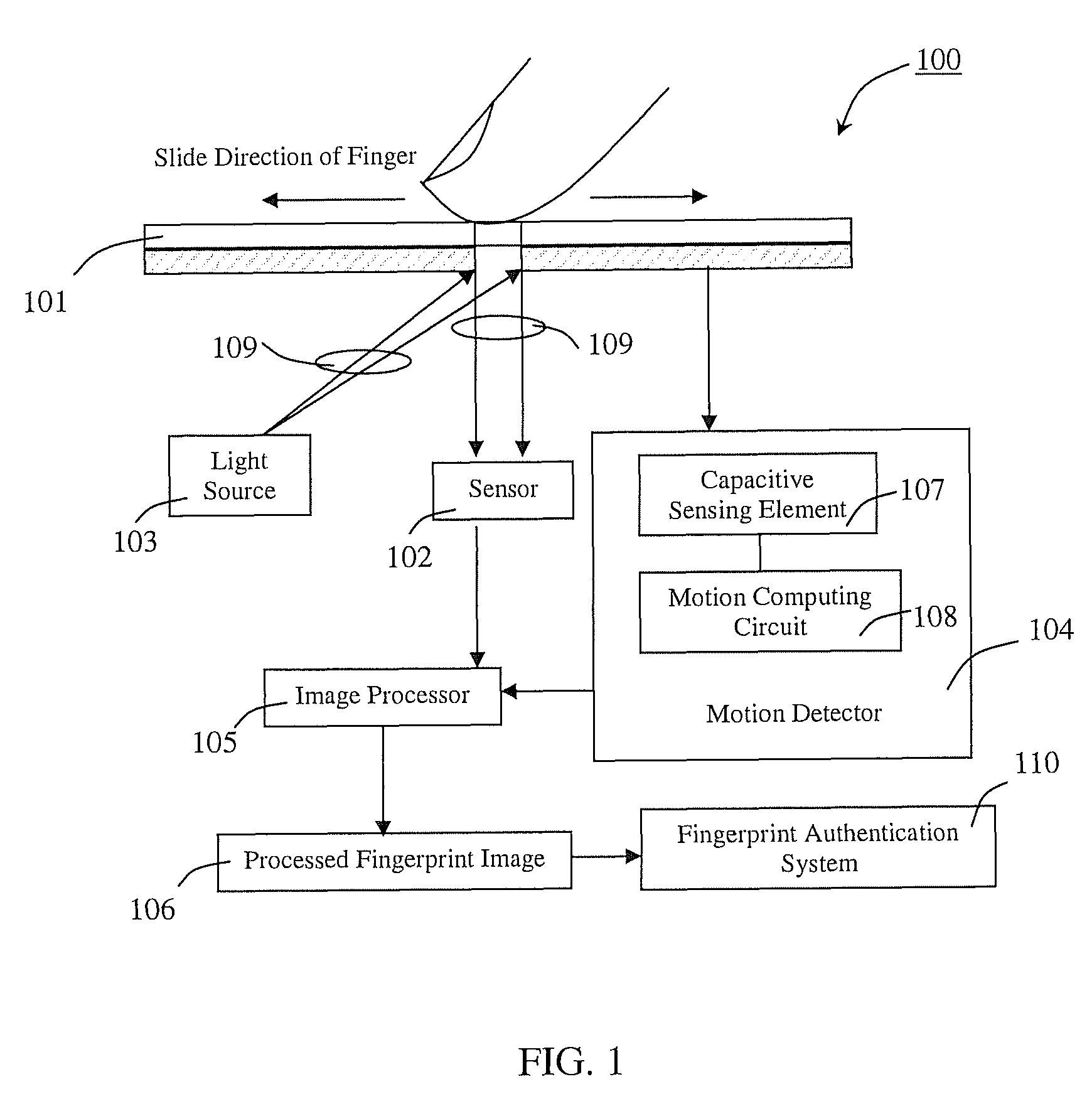
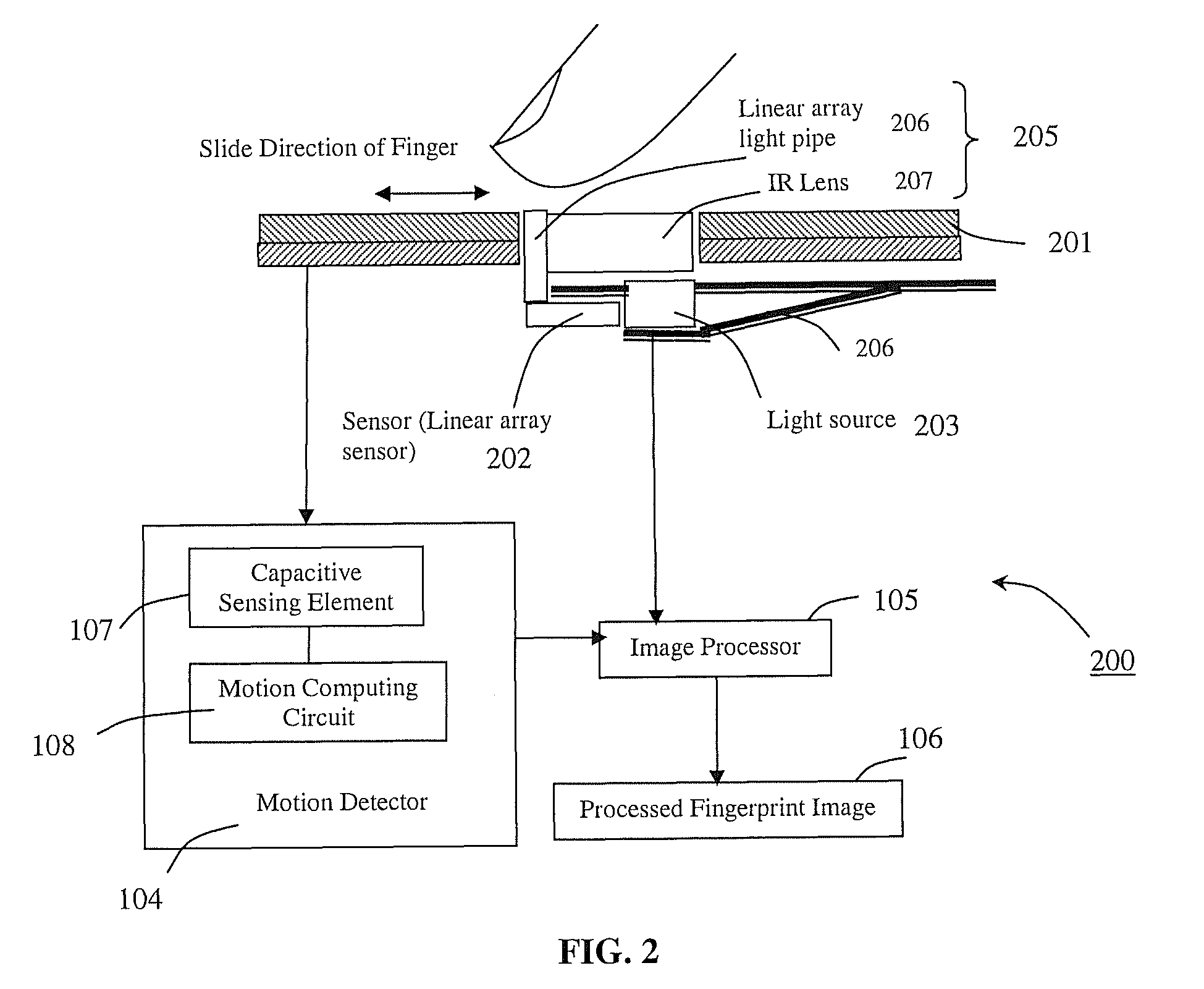
[0013]FIG. 1 depicts a schematic block diagram of one embodiment of a fingerprint sensing device 100 with a touch sensitive surface 101 for users to place or slide a finger over the touch sensitive surface 101 for subsequently generating a fingerprint image. In one embodiment, the fingerprint sensing device 100 includes a sensor 102, a light source 103, a capacitive based motion detector 104 and an image processor 105. Although certain components or elements are illustrated in conjunction with the fingerprint sensing device 100 of FIG. 1, other embodiments may include more or fewer components, or any equivalent components which is capable of providing a similar or even a more complex fingerprint sensing function. For example, some embodiments of fingerprint sensing device may include a circuitry embedded therein and or incorporated within the sensor to process the fingerprint image and at the same time may provide other function such as optical finger navigation as will be appreciat...


PUM


Abstract

A fingerprint sensing module for a touch screen device. The fingerprint sensing module includes a sensor, a light source, a motion detector, and an image processor. The sensor sets to capture portions for a fingerprint image as a finger is slid over the sensor. The motion detector determines a rate of the finger movement as the finger is slide over the touch screen device. The image processor reads fingerprint images from the sensor and the fingerprint motion data from the motion detector. The image processor subsequently combines portions of the fingerprint images into a complete fingerprint in accordance with the rate of the finger's movement.

Description

BACKGROUND OF THE INVENTION[0001]Fingerprint sensing devices have been widely used for security systems and fingerprint authentication. A typical fingerprint sensing device includes some form of a sensor for generating a representation of a fingerprint of a finger that is placed over or in direct contact with the sensor. In general, fingerprint detection methods may be capacitive, thermal, optical and ultrasonic; wherein the sensor captures the fingerprint image when a finger is either statically placed on the surface of the sensor or slid over the sensor surface.[0002]More recently, electronic devices such as computers, and portable electronic devices like cell phones, have incorporated a fingerprint detector for individual authentication for security and data protection. For such devices, a main challenge is the size of the sensor, since it is more desirable to have a sensor with a small footprint. In addition, product reliability and system robustness are also key requirements.[0...

Claims


Application Information

Patent Timeline
Patent Type & Authority Patents(United States)
IPC IPC(8): G06K9/00
CPCG06F3/0421G06F3/044G06F3/0488G06K9/00026G06F2203/0338G06V40/1335A61B5/117H04B1/38G06F18/00
Inventor ORSLEY, TIMOTHY JAMES
Owner AVAGO TECH INT SALES PTE LTD
Learn More