
Multipoint nanostructure-film touch screen

a nanostructure, touch screen technology, applied in the field of electronic devices, can solve the problems of high-temperature sputtering, high cost of ito deposition, and many are only capable of reporting a single elemen

Active Publication Date: 2013-11-19
SAMSUNG ELECTRONICS CO LTD
View PDF15 Cites 14 Cited by
  • Summary
  • Abstract
  • Description
  • Claims
  • Application Information

AI Technical Summary

Problems solved by technology

However, ITO can be an inadequate solution for many of the above-mentioned applications (e.g., due to its relatively brittle nature, correspondingly inferior flexibility and abrasion resistance), and the indium component of ITO is rapidly becoming a scarce commodity.
Additionally, ITO deposition usually requires expensive, high-temperature sputtering, which can be incompatible with many device process flows.
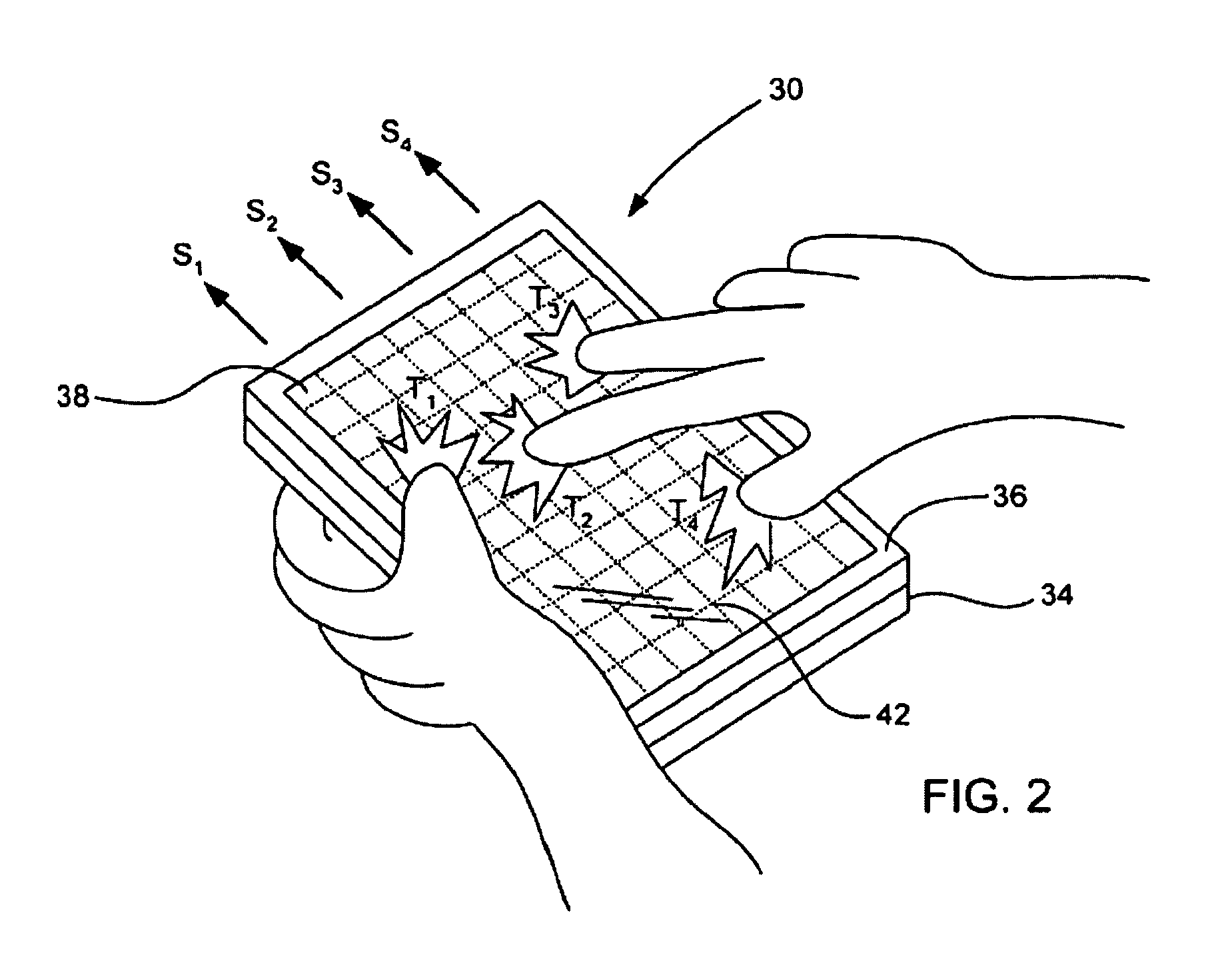
One problem found in conventional touch screen technologies is that many are only capable of reporting a single point even when multiple objects are placed on the sensing surface.
That is, they lack the ability to track multiple points of contact simultaneously.
In surface wave and infrared technologies, it is difficult, if not impossible, to discern the exact position of multiple touch points that fall on the same horizontal or vertical lines due to masking.
In either case, faulty results are generated.
A related problem found in many conventional touch screen technologies is that they utilize transparent conductive materials that are ill-suited for touch panel functionality.
For example, ITO can be an inadequate touch panel solution, given that ITO is relatively brittle and consequently prone to mechanical degradation, in which case faulty results are generated.
Additionally, currently-available ITO deposition methods can be limiting in terms of the possible touch screen device architectures enabled thereby.

Method used


Image

  • Multipoint nanostructure-film touch screen
  • Multipoint nanostructure-film touch screen
  • Multipoint nanostructure-film touch screen

Examples


Embodiment Construction

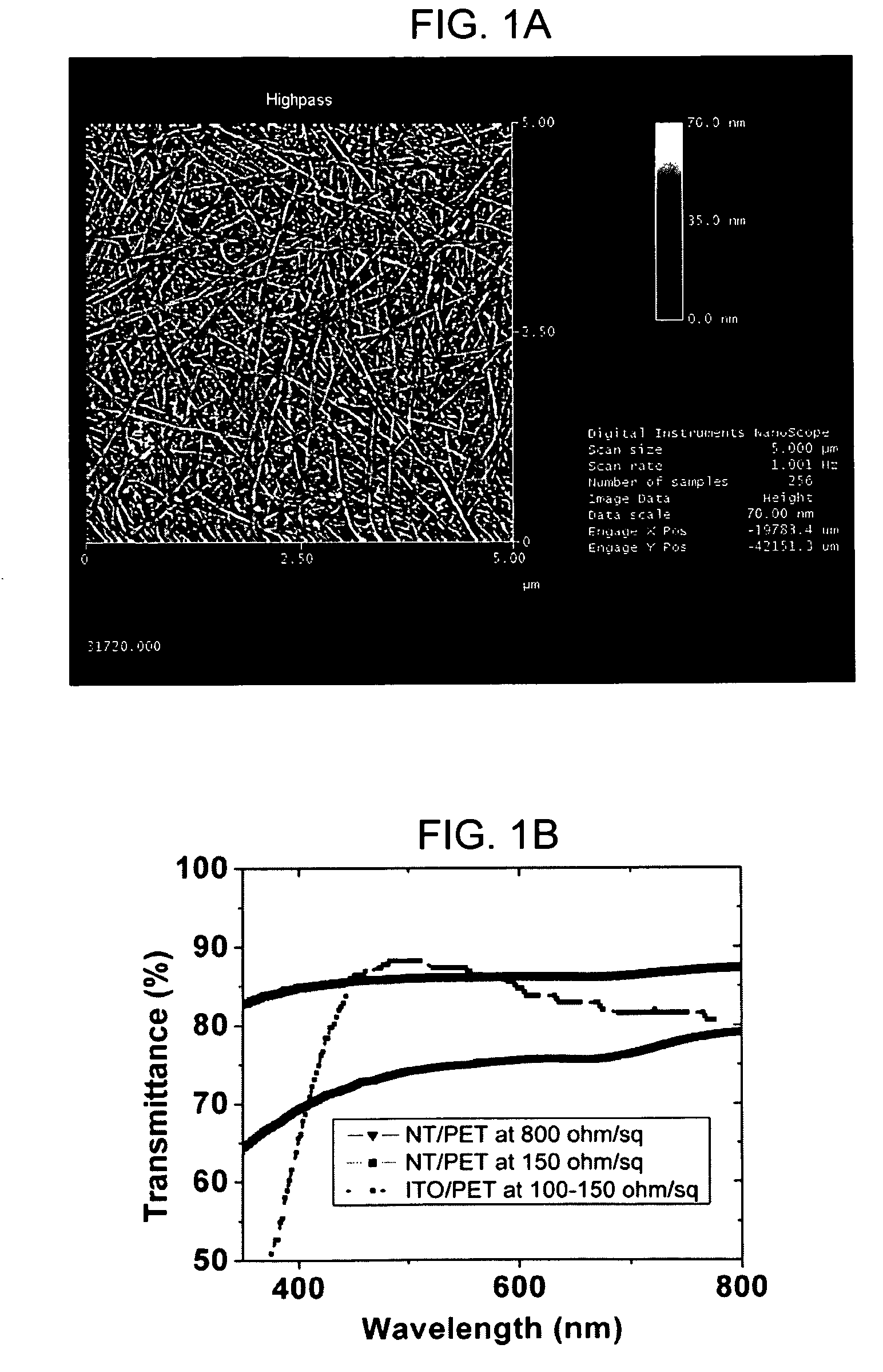
[0040]Referring to FIG. 1, a nanostructure film according to one embodiment of the present invention comprises at least one interconnected network of single-walled carbon nanotubes (SWNTs). Such film may additionally or alternatively comprise other nanotubes (e.g., MWNTs, DWNTs), other fullerenes (e.g., buckyballs), graphene flakes / sheets, and / or nanowires (e.g., metallic (e.g., Ag, Ni, Pt, Au), semiconducting (e.g., InP, Si, GaN), dielectric (e.g., SiO2, TiO2), organic, inorganic).

[0041]Such nanostructure film may further comprise at least one functionalization material bonded to the nanostructure film. For example, a dopant bonded to the nanostructure film may increases the electrical conductivity of the film by increasing carrier concentration. Such dopant may comprise at least one of Iodine (I2), Bromine (Br2), polymer-supported Bromine (Br2), Antimonypentafluride (SbF5), Phosphoruspentachloride (PCl5), Vanadiumoxytrifluride (VOF3), Silver(II) Fluoride (AgF2), 2,1,3-Benzoxadiazo...


PUM


Abstract

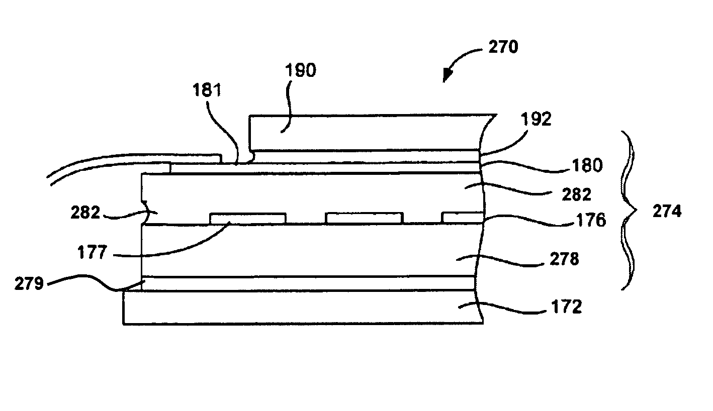
A touch screen comprising at least one nanostructure film and capable of detecting multiple touches occurring at the same time at distinct locations in a plane of the touch screen is described. The touch screen may comprise a sensing layer, a driving layer and / or a shielding layer. At least one of these layers may comprise a nanostructure film, and at least two of these layers may be formed on a common substrate.

Description

[0001]This application claims priority to U.S. Provisional Application No. 60 / 976,235, filed Sep. 28, 2007 and entitled “MULTIPOINT NANOSTRUCTURE-FILM TOUCH SCREEN,” the entire contents of which are hereby incorporated herein by reference.FIELD OF THE INVENTION[0002]The present invention relates generally to an electronic device having a touch screen comprising at least one nanostructure film. More particularly, the present invention relates to a nanotube-film touch screen capable of sensing multiple points at the same time.BACKGROUND OF THE INVENTION[0003]Many modern and / or emerging applications require at least one device electrode that has not only high electrical conductivity, but high optical transparency as well. Such applications include, but are not limited to, touch screens (e.g., analog, resistive, 4-wire resistive, 5-wire resistive, surface capacitive, projected capacitive, multi-touch, etc.), displays (e.g., flexible, rigid, electro-phoretic, electro-luminescent, electro...

Claims


Application Information

Patent Timeline
Patent Type & Authority Patents(United States)
IPC IPC(8): G06F3/042
CPCG06F3/041G06F2203/04808G06F3/0443G06F3/0445G06F3/0446G06F2203/04104G06F3/04166
Inventor GANDHI, SHRIPALTHOMAS, DAVID
Owner SAMSUNG ELECTRONICS CO LTD
Learn More