
Method and apparatus for management of over-erasure in NAND-based NOR-type flash memory

a flash memory and nand-based technology, applied in static storage, digital storage, instruments, etc., can solve the problems of flash nonvolatile memory cell over-erasure, small current may leak through the memory cell, and the number of its required external pins increases by one, so as to achieve sufficient magnitude and duration, the effect of long duration

Inactive Publication Date: 2013-11-12
APLUS FLASH TECH
View PDF7 Cites 7 Cited by
  • Summary
  • Abstract
  • Description
  • Claims
  • Application Information

AI Technical Summary

Benefits of technology

[0015]Another object of this invention is to provide a method and apparatus for erasing dual charge retaining transistor NOR flash memory cells to set a threshold voltage level of the erased dual charge retaining transistor NOR flash memory cells to prevent leakage current from corrupting data during a read or verification operation.
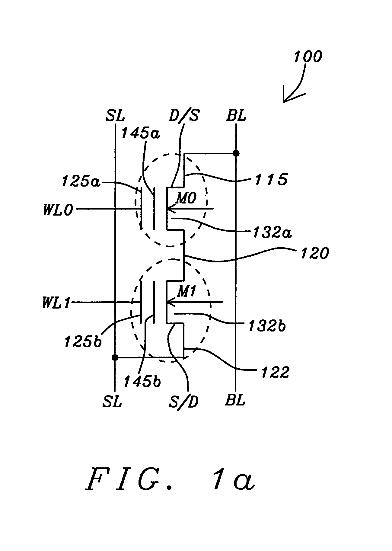
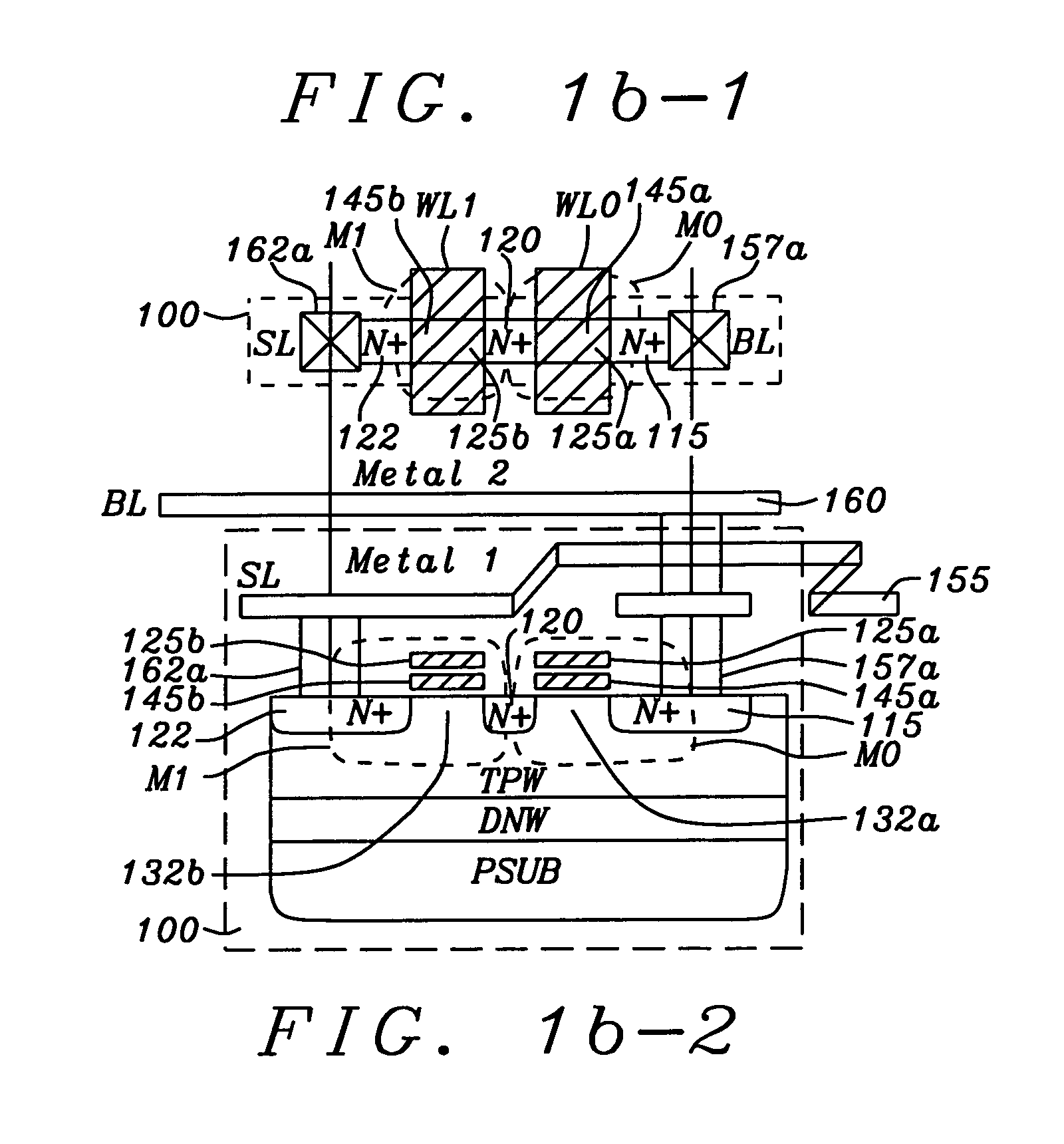
[0030]The column voltage control circuit has a well bias control circuit that includes a shallow well generator and a deep well generator. The deep well generator is connected to a deep diffusion well of a first conductivity type (N-type) that is diffused into a surface of the substrate. A shallow diffusion well of a second conductivity type (P-type) is diffused into the deep diffusion well of the first conductivity type. The shallow diffusion well of the second conductivity type is connected to the shallow well generator. The deep well generator generates a voltage level of the power supply voltage source for programming, verification, and reading of the array of NOR flash memory cells and generates a very large erase voltage during the erasing a selected block or a page of the array of NOR flash memory cells. The shallow well generator transfers the voltage level of the ground reference voltage source (0.0V) for programming, verification, and reading of the array of NOR flash memory cells. The shallow well generator generates a very large erase voltage level that is applied to the shallow well of the second conductivity type to attract the charges from the charge retaining region during an erase. The very large erase voltage that is generated by the deep well generator and the shallow well generator prevent undesired forward currents between the deep diffusion well and the shallow diffusion well.

Problems solved by technology

One disadvantage of NOR flash nonvolatile memory is as the density is doubled, the number of its required external pin count increases by one due to the adding of one more external address pin to double the address space.
However, a Flash nonvolatile memory cell suffers from the problem of over-erasure.
This biases the memory cell slightly on, so that a small current may leakage through the memory cell even when it is not addressed.
However, not all of the Flash memory cells of the Flash memory array have the same circuit characteristics.
This leakage current causes the data reading accuracy of the Flash memory array to be adversely affected.
The bit line will suffer from excess leakage current while reading the non-conducting Flash memory cell.

Method used


Image

  • Method and apparatus for management of over-erasure in NAND-based NOR-type flash memory
  • Method and apparatus for management of over-erasure in NAND-based NOR-type flash memory
  • Method and apparatus for management of over-erasure in NAND-based NOR-type flash memory

Examples


Embodiment Construction

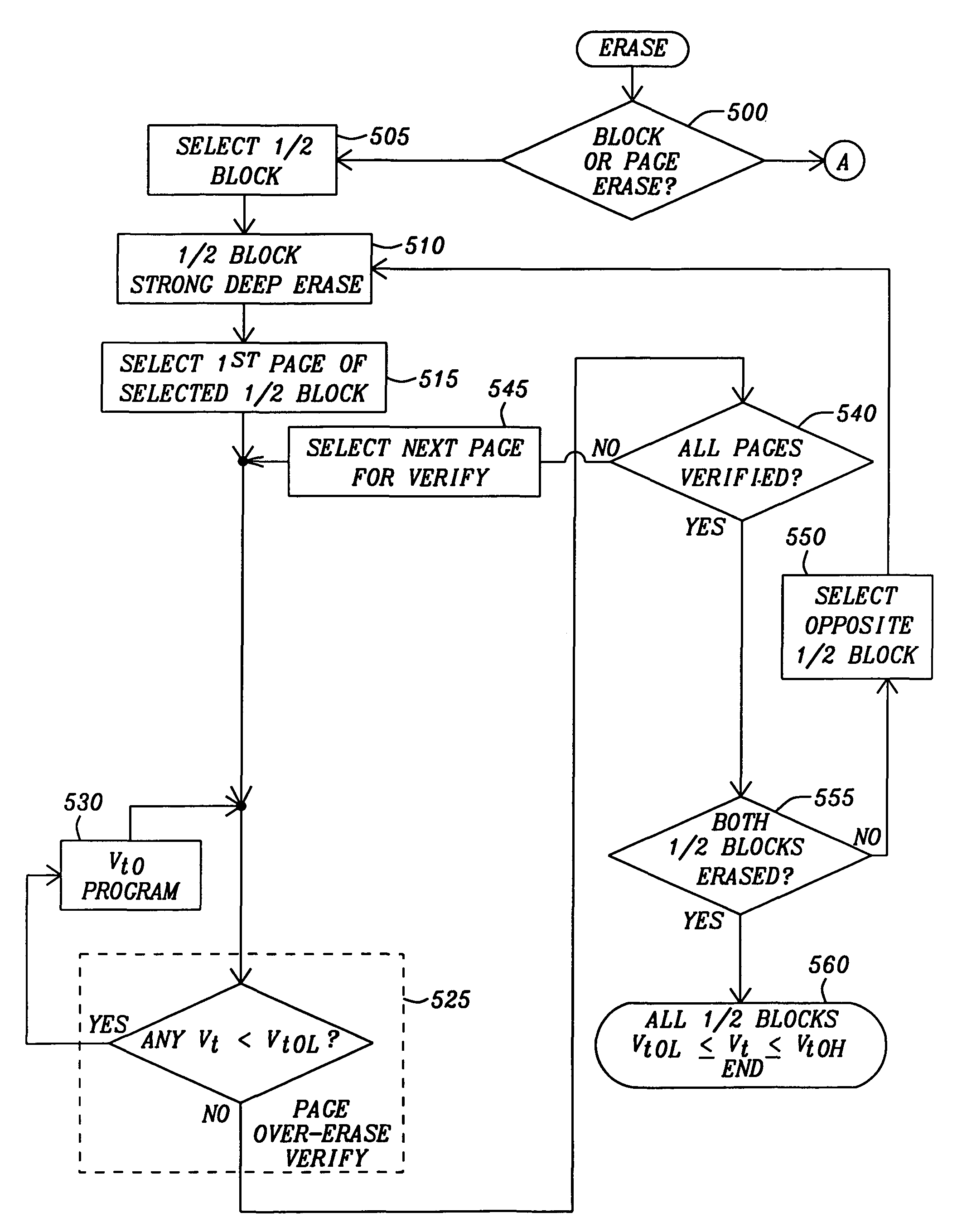
[0051]As described above, over-erasure occurs if, during the erasing step, too many electrons are removed from the floating gate leaving a slight positive charge. This biases the dual floating gate transistor NOR flash memory cell to be conducting such that a current may leak through the dual floating gate transistor NOR flash memory cell even when it is not addressed. To eliminate over-erasing in an array of the NAND-like dual charge retaining transistor NOR flash memory cells, erasure of a block of dual charge retaining (charge storage in a floating gate or charge trapping in a SONOS (silicon-oxide-nitride-oxide silicon)) NOR flash memory cells begins by selecting a first half block of alternating pages of charge retaining transistors. A block of the array of dual charge retaining transistor NOR flash memory cells has two half blocks where each half blocks includes the pages of alternating rows of the dual charge retaining transistor NOR flash memory cells. The dual charge retaini...


PUM


Abstract

A method and apparatus for operating an array block of dual charge retaining transistor NOR flash memory cells by erasing the dual charge retaining transistor NOR flash memory cells to set their threshold voltage levels to prevent leakage current from corrupting data during a read operation. Erasure of the array block of NOR flash memory cells begins by selecting one of block section of the array block and strongly and deeply erasing, over-erase verifying, and programming iteratively until the charge retaining transistors have their threshold voltages between the lower voltage limit and the upper voltage limit of the first program state. Other block sections are iteratively selected and erased, over-erase verified, and programmed repeatedly until the charge retaining transistors have their threshold voltages between the lower voltage limit and the upper voltage limit of the first program state until the entire block has been erased and reprogrammed to a positive threshold level.

Description

RELATED PATENT APPLICATIONS[0001]U.S. patent application Ser. No. 12 / 658,121, filed on Feb. 3, 2010, assigned to the same assignee as the present invention, and incorporated herein by reference in its entirety.[0002]U.S. patent application Ser. No. 12 / 387,771, filed on May 7, 2009, assigned to the same assignee as the present invention, and incorporated herein by reference in its entirety.[0003]U.S. patent application Ser. No. 12 / 455,337, filed on Jun. 1, 2009, assigned to the same assignee as the present invention, and incorporated herein by reference in its entirety.BACKGROUND OF THE INVENTION[0004]1. Field of the Invention[0005]This invention relates generally to nonvolatile memory array structures and operation of the nonvolatile memory array structures. More particularly, this invention relates to methods and apparatus for the operation of a dual charge retaining transistor NOR nonvolatile memory device structures.[0006]2. Description of Related Art[0007]Nonvolatile memory is w...

Claims


Application Information

Patent Timeline
Patent Type & Authority Patents(United States)
IPC IPC(8): G11C11/34
CPCG11C16/3409G11C16/3445G11C16/0458G11C16/3459G11C11/5635G11C11/5628G11C16/08G11C16/24G11C2211/5621
Inventor LEE, PETER WUNG
Owner APLUS FLASH TECH
Learn More