
Communication system and method

a communication system and communication technology, applied in the field of communication techniques, can solve the problems of inability to achieve the high speed of i/o logic, inability to manufacture a single process, and severe limitations in the design of complex systems within an integrated circuit, so as to improve the use of communication bandwidth and improve the use of bandwidth

Active Publication Date: 2013-11-05
STMICROELECTRONICS (GRENOBLE 2) SAS +1
View PDF7 Cites 5 Cited by
  • Summary
  • Abstract
  • Description
  • Claims
  • Application Information

AI Technical Summary

Benefits of technology

This approach enhances bandwidth usage by optimizing the transmission of data packets and virtual wires, reducing latency, and enabling efficient communication between integrated circuits with different technological nodes, achieving a bandwidth gain of 35 GB / s and improving hardware implementation.

Problems solved by technology

However, said improvement does not extend directly to the analog or input / output (I / O) cells, which leads to severe limitations during design of complex systems within an integrated circuit such as Systems-on-Chip (SoCs).
Furthermore, when a technology with small feature size is used, for example a sub32-nm technology, a high speed of the I / O logic can, in some cases, only be achieved with a low supply voltage.
However, complex circuits can also comprise communication interfaces with higher voltages, for example a communication interface of the “High-Definition Multimedia Interface” (HDMI) type, of the “Serial Advanced Technology Attachment” (SATA) type, or of the “Universal Serial Bus” version 3 (USB3) type.
For instance, in one case, the communication interface of the DDR3 memory forms a gate oxide with a thickness of 30 Å, whereas the HDMI communication interface would form a thickness of 50 Å. However, this case cannot be obtained with a single manufacturing process.

Method used


Image

  • Communication system and method
  • Communication system and method
  • Communication system and method

Examples


Embodiment Construction

[0033]Illustrated in the ensuing description are various specific details aimed at providing an in-depth understanding of the embodiments. The embodiments can be obtained without one or more of the specific details, or with other methods, components, materials, etc. In other cases, known structures, materials, or operations are not illustrated or described in detail so that various aspects of the embodiments will not be obscured.

[0034]The reference to “an embodiment” or “one embodiment” in the framework of the present description is intended to indicate that a particular configuration, structure, or characteristic described in relation to the embodiment is comprised in at least one embodiment. Hence, phrases such as “in an embodiment” and “in one embodiment,” which may be present in different points of this description, do not necessarily refer to one and the same embodiment. Furthermore, particular conformations, structures, or characteristics can be combined adequately in one or m...


PUM


Abstract

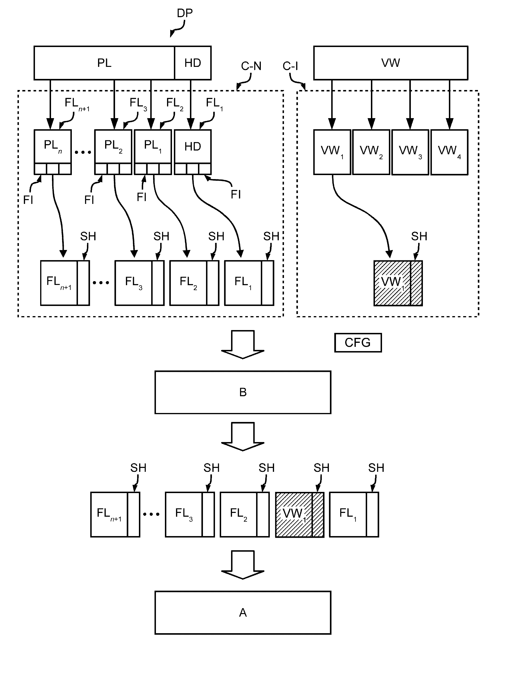
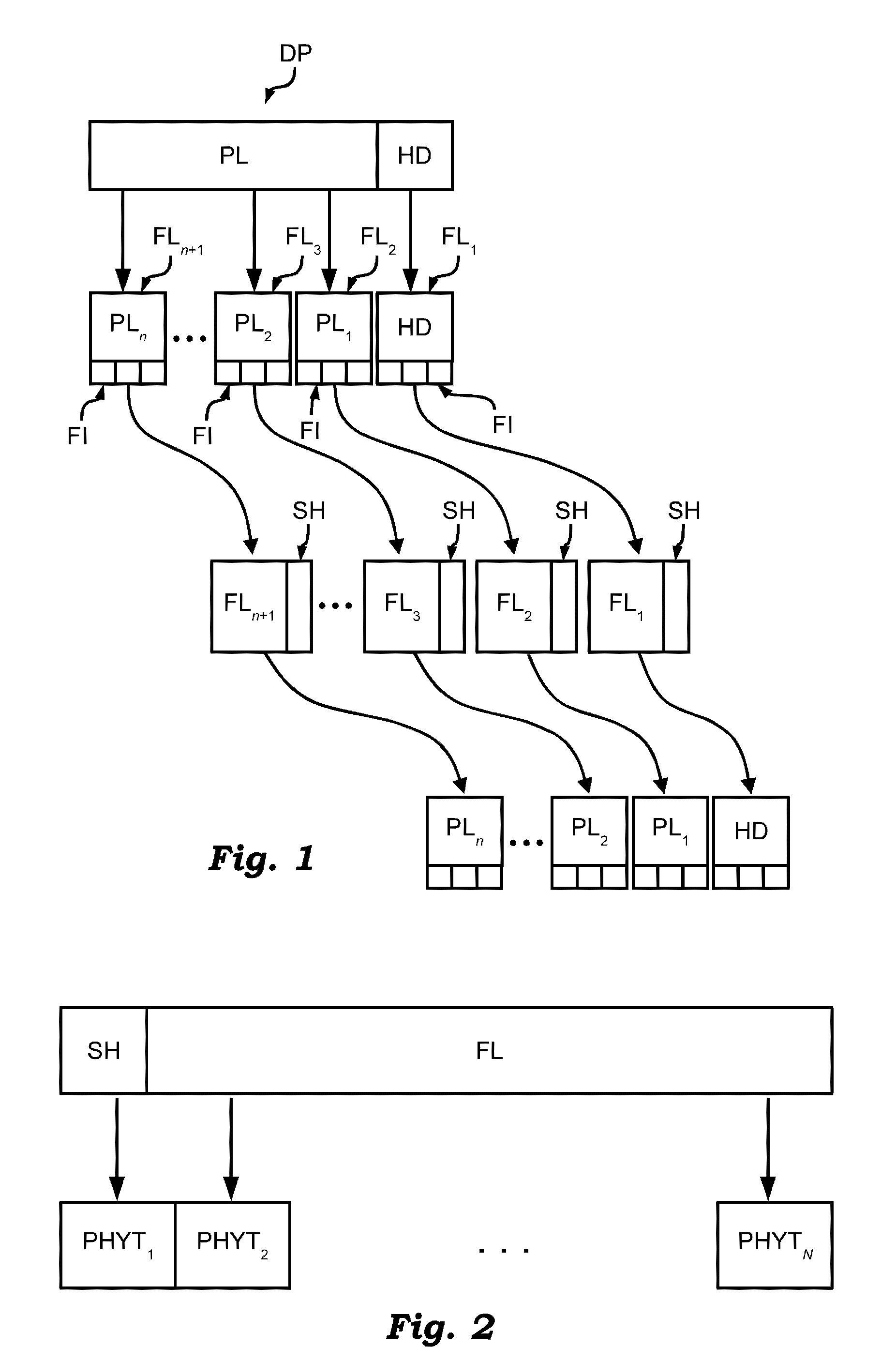
A communication system for transmitting data, for example, within a System-in-Package. The system includes a first circuit configured for: a) dividing the data into a plurality of packets having a determined size; and b) creating for each of the packets a transmission segment including a segment header and the respective packet as payload. The system also includes a second circuit configured for: a) separating the transmission segments into a plurality of physical units, where the physical units have a determined size; and b) transmitting the physical units over a physical communication channel. In particular, the segment header includes at least one field that identifies the number of physical units that are to be transmitted.

Description

BACKGROUND[0001]1. Technical Field[0002]The present disclosure relates to communication techniques.[0003]The disclosure has been developed with particular attention paid to its possible use in the so-called Network-in-Package (NiP) architectures, such as the ones used for communication between different circuits integrated within a System-in-Package (SiP) that require a high level of performance.[0004]2. Description of the Related Art[0005]Systems-in-Package (SiPs) are heterogeneous electronic systems that comprise a plurality of integrated circuits. For instance, said integrated circuits are frequently mounted directly as dice in a common package and communicate with one another via a network for communication within the package, referred to as Network-in-Package (NiP).[0006]For instance, such SiPs are particularly useful for interfacing integrated circuits that have been produced with different manufacturing processes.[0007]For instance, the improvement of the processes for manufa...

Claims


Application Information

Patent Timeline
Patent Type & Authority Patents(United States)
IPC IPC(8): H04J3/24
CPCG06F13/42
Inventor SCANDURRA, ALBERTOGUARNACCIA, GIUSEPPEURZI', IGNAZIO ANTONINO
Owner STMICROELECTRONICS (GRENOBLE 2) SAS
Learn More