


Quick Research
Generate reliable direction feasibility study reports for your R&D in just a few steps.

Technical Q&A
Discover and master advanced knowledge NOW. Basics, ideas, possibilities, all at once.

Find Solutions
As an expert in R&D theories, this can generate solutions to your technical problems instantly.

Evaluate Feasibility
Analyze your overall solution with one click, know your potential R&D risks in advance.

Monitor Landscape
Get weekly tech updates, stay abreast of the latest tech innovations and key insights.
Methods for controlling the crystalline nanofibre content of organic layers used in organic electronic devices
a technology of organic electronic devices and nanofibers, which is applied in the field of organic electronics, can solve the problems of labor-intensive and tedious control of nanofiber content using this method, and achieve the effect of convenient and quick
- Summary
- Abstract
- Description
- Claims
- Application Information
AI Technical Summary
Benefits of technology
Problems solved by technology
Method used
Image

Examples
example 1
Preparation of a Mother Polymer Dispersion Based on P36T
[0147]5 mg of regioregular poly(3-hexylthiophene) having a Mn of 23700 g / mol and a Mw of 42700 g / mol [determined relative to poystyrene standards in chlorobenzene at 60° C.] were dissolved in 10 g of heated cyclohexanone at 150° C. under agitation until total dissolution of the polymer (clear orange solution).
[0148]This dissolution corresponds to the step (a) of forming a solution by dissolving a nanofibre-forming polymer in a solvent at a temperature T1 high enough to enable the formation of said solution.
[0149]During the process of dissolution, the solution was protected from light and air, to avoid chemical oxidation and / or photo-oxidation. After the total dissolution of the nanofibre-forming polymer, the solution was slowly cooled to 50° C. The speed of cooling was approximately 20° C. / hour. At 50° C. the solution was filtered through a porous membrane (typically a teflon® filter membrane with a 0.45 μm porosity) to remove ...
example 2
Preparation of Polymer Dispersions Based on Regioregular P3mT with Adjustable Nano-Fiber Contents According to an Embodiment of the Present Invention
[0151]Mother Polymer dispersions were made according to example 1 but choosing from 25 solvents and 7 polymers of the general formula (I):
[0152]
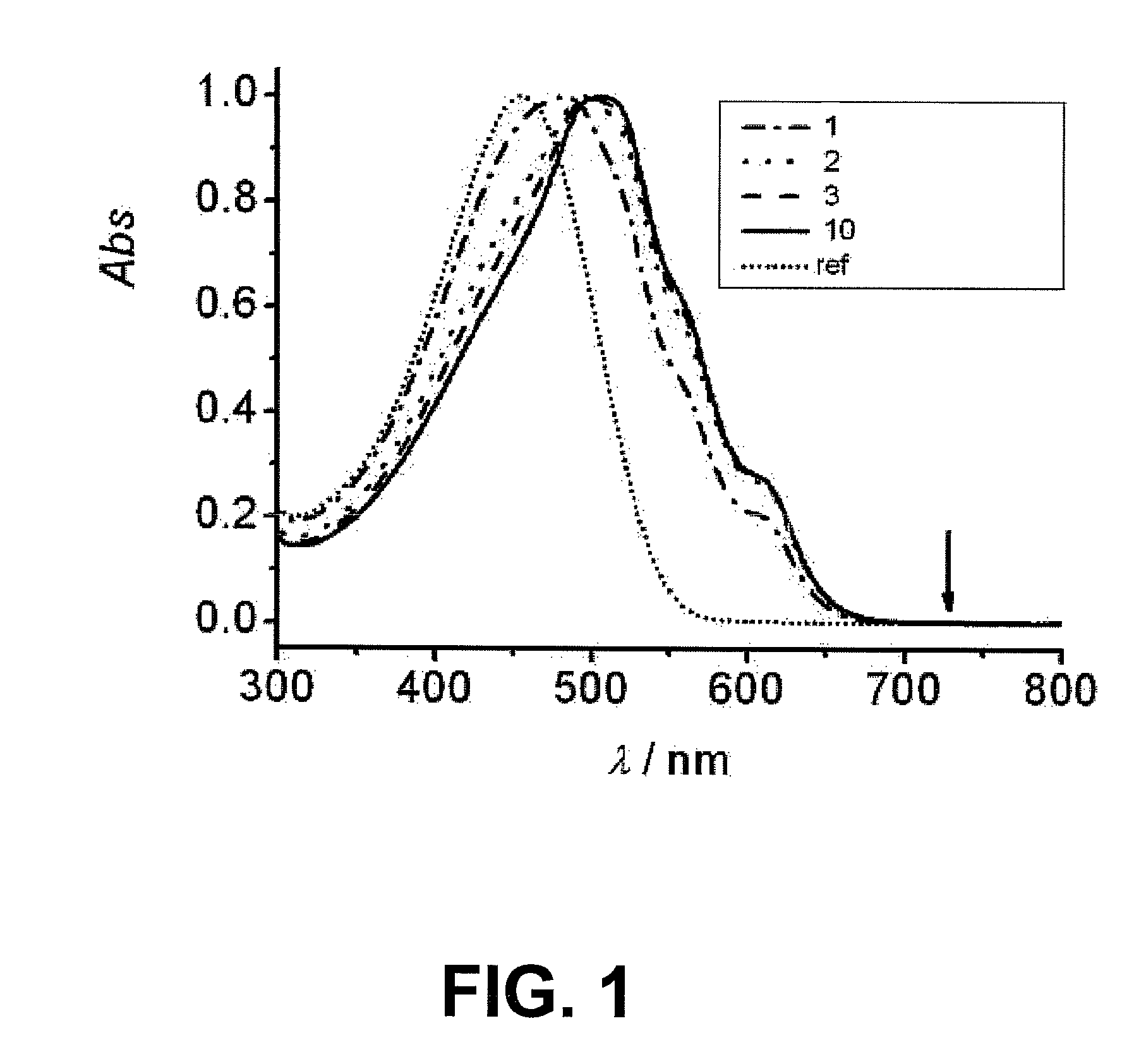
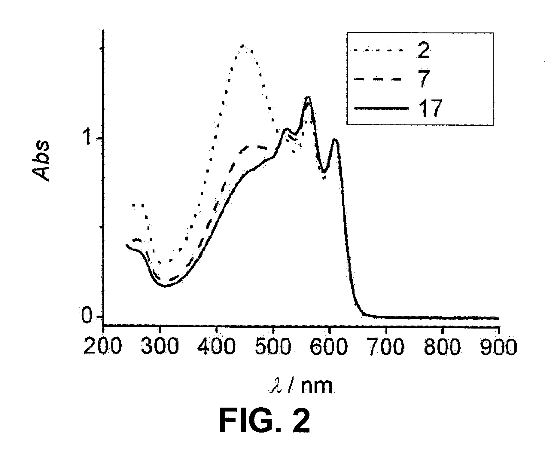
wherein R is a linear alkyl chain having from 3 to 9 carbon atoms. The 61 combinations solvent / polymer (see table below wherein m indicates the number of carbon atoms in the R group) were tested for various concentrations of polymer (I) (from 0.001 wt % to 5 wt %, see FIG. 4) and dispersions comprising crystalline nanofibres of the nanofibre-forming polymer (I) were obtained without aggregates upon cooling as described for example 1. In FIG. 4, curves 1 to 6 relates respectively to the use of the following solvents: tetralin, 1,2,4-trimethylbenzene, p-xylene, decaline, chorobenzene and cyclohexanone; the integer n (X-axis) indicates the number of carbons in the R chain; the Y-axis indicates the ...
example 3
Preparation of a Polymer Composition with Different Nano-Fiber Contents in Active Layers (General Procedure)
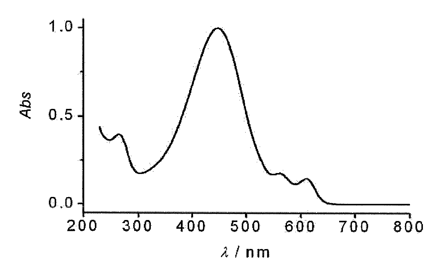
[0159]Polymer compositions were made by adding PCBM to the wanted mother polymer dispersion obtained in accordance with example 2, in this example P3alkylT:PCBM in a pre-defined weight ratio. These polymer compositions were stirred with a magnetic stirrer for 2 days at room temperature. Then the polymer composition was put in a heating block under continuously stirring and heated until a temperature T3 above 20° C. was reached. The solution was left for at least one hour at this temperature T3 (to obtain a new fibre content equilibrium). A very small amount of the polymer composition at the temperature T3 (about 45 μl) was taken and diluted in about 3 ml of solvent in order to determine the exact crystalline nanofibre content of the polymer composition by UV-Vis or by GPC.
[0160]Then about 300 μl to 400 μl of the solution was spin-coated to make an active layer from the polymer...
PUM
| Property | Measurement | Unit |
|---|---|---|
| temperature T1 | aaaaa | aaaaa |
| temperature T1 | aaaaa | aaaaa |
| temperature T1 | aaaaa | aaaaa |
Abstract
Description
Claims
Application Information
 - R&D Engineer
- R&D Manager
- IP Professional
- Industry Leading Data Capabilities
- Powerful AI technology
- Patent DNA Extraction
Browse by: Latest US Patents, China's latest patents, Technical Efficacy Thesaurus, Application Domain, Technology Topic, Popular Technical Reports.
© 2024 PatSnap. All rights reserved.Legal|Privacy policy|Modern Slavery Act Transparency Statement|Sitemap|About US| Contact US: help@patsnap.com