Light-emitting device
a technology of light-emitting diodes and diodes, which is applied in the direction of semiconductor devices, basic electric elements, electrical apparatus, etc., can solve the problems of difficult to raise the light efficiency of light-emitting diodes, and achieve the effect of reducing the opportunity of light and raising the light extraction efficiency
- Summary
- Abstract
- Description
- Claims
- Application Information
AI Technical Summary
Benefits of technology
Problems solved by technology
Method used
Image
Examples
first embodiment
[0025]FIG. 2 is a schematic illustration of the structure in accordance with the present application. As shown in FIG. 2, the light-emitting diode device 200 of this embodiment includes a substrate 20, an epitaxial structure 22 formed on the substrate 20 wherein the epitaxial structure includes a first-type conductivity cladding layer 220, a first-type conductivity confining layer 222, a light-emitting layer 224, a second-type conductivity confining layer 226, and a second-type conductivity cladding layer 228 epitaxially grown from the bottom to the top. Besides, a least an electrode is formed on the epitaxial structure 22 wherein the thickness of the first-type conductivity confining layer 222 T1 is not equal to the thickness of the second-type conductivity confining layer 226 T2. The thickness ratio T1 / T2 of the first-type conductivity confining layer 222 T1 and the second-type conductivity confining layer 226 T2 is ½˜ 1 / 200 or 2-200. In a preferred embodiment, the thickness ratio...
second embodiment
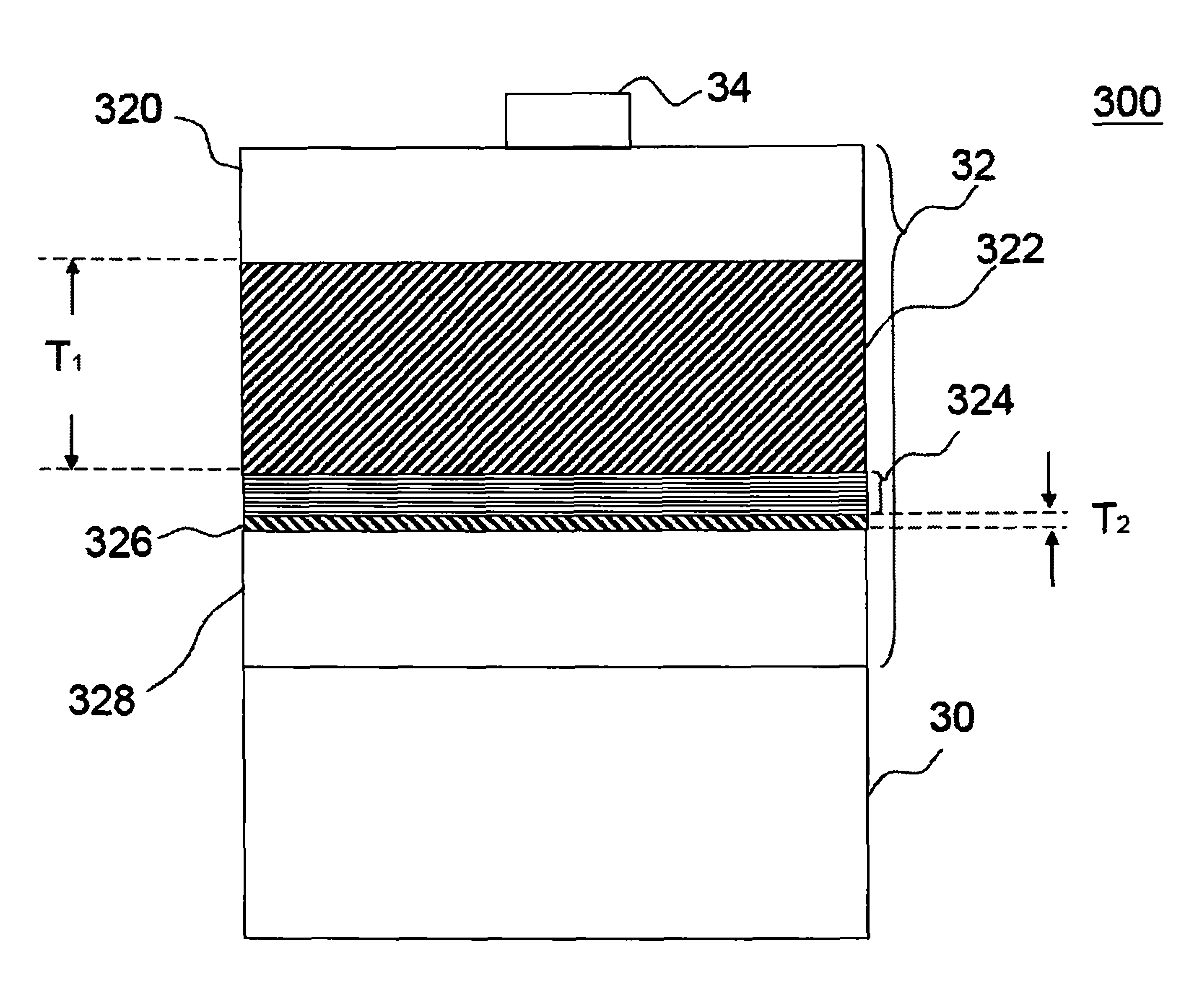
[0027]FIG. 4 is a schematic illustration of the structure in accordance with the present application. As shown in FIG. 4, the light-emitting diode device 300 of this application includes a substrate 30, an epitaxial structure 32 formed on the substrate 30 and a least an electrode 34 formed on the epitaxial structure 32. The epitaxial structure a least includes a first-type conductivity cladding layer 320, a first-type conductivity confining layer 322, a light-emitting layer 324, a second-type conductivity confining layer 326, and a second-type conductivity cladding layer 328 epitaxially grown from the bottom to the top. The material of the substrate is chosen form the material having the characteristic of high thermal conduction, high transparency, high reflection, or high electrical conduction. Besides, in this embodiment, the thickness of the first-type conductivity confining layer 322 T1 is about 500 nm, and the thickness of the second-type conductivity confining layer 326 T2 is ...
PUM
 Abstract
Description
Claims
Application Information
 - R&D Engineer
- R&D Manager
- IP Professional
- Industry Leading Data Capabilities
- Powerful AI technology
- Patent DNA Extraction
Browse by: Latest US Patents, China's latest patents, Technical Efficacy Thesaurus, Application Domain, Technology Topic, Popular Technical Reports.
© 2024 PatSnap. All rights reserved.Legal|Privacy policy|Modern Slavery Act Transparency Statement|Sitemap|About US| Contact US: help@patsnap.com


