Display apparatus and electronic apparatus
a technology of electronic equipment and display apparatus, which is applied in the field of display equipment and electronic equipment, can solve problems such as the difficulty of compensating for a current variation in a correction process or a similar process, and achieve the effect of suppressing the unevenness of illumination
- Summary
- Abstract
- Description
- Claims
- Application Information
AI Technical Summary
Benefits of technology
Problems solved by technology
Method used
Image
Examples
embodiment
1. Embodiment
System Configuration
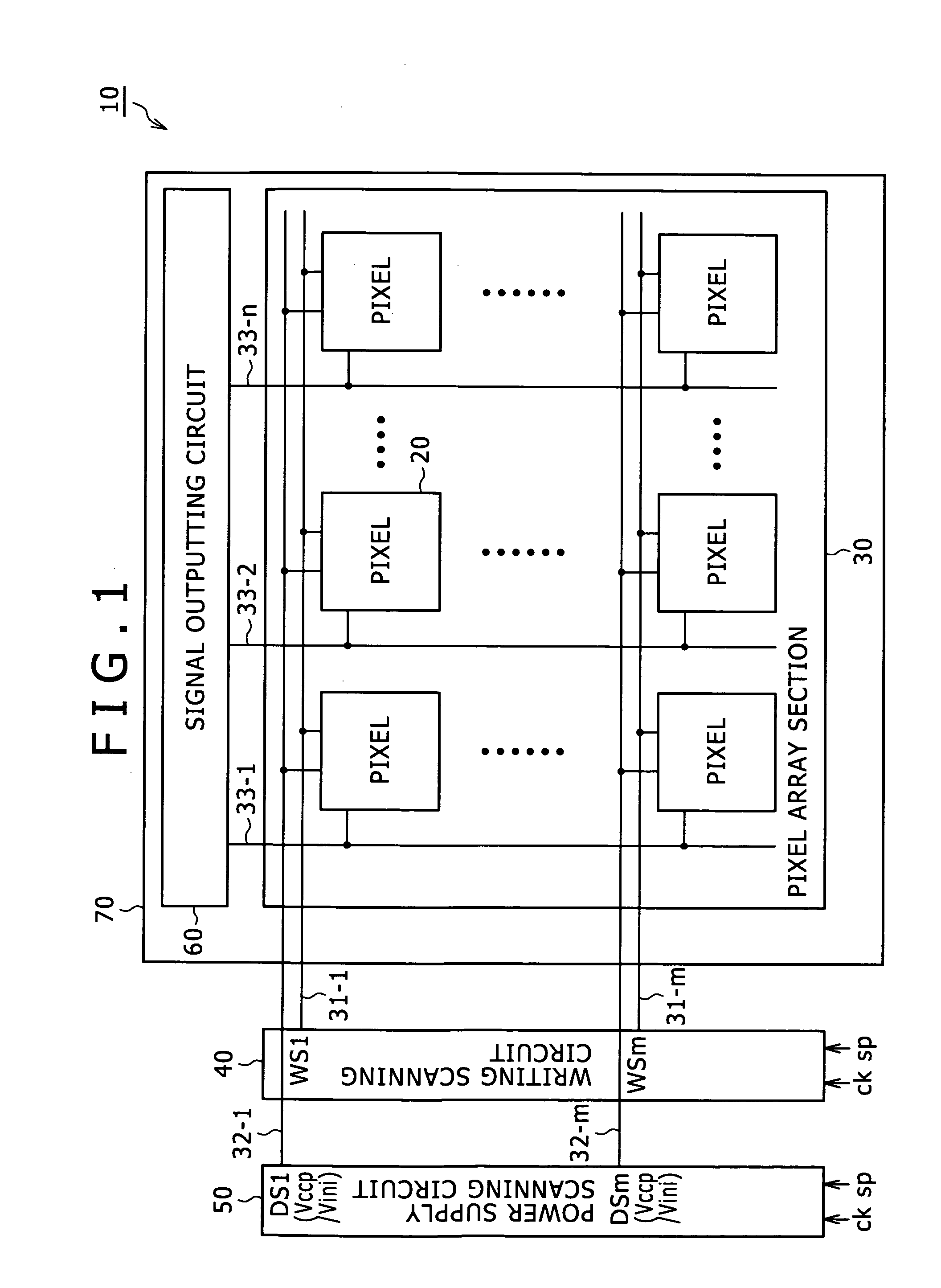
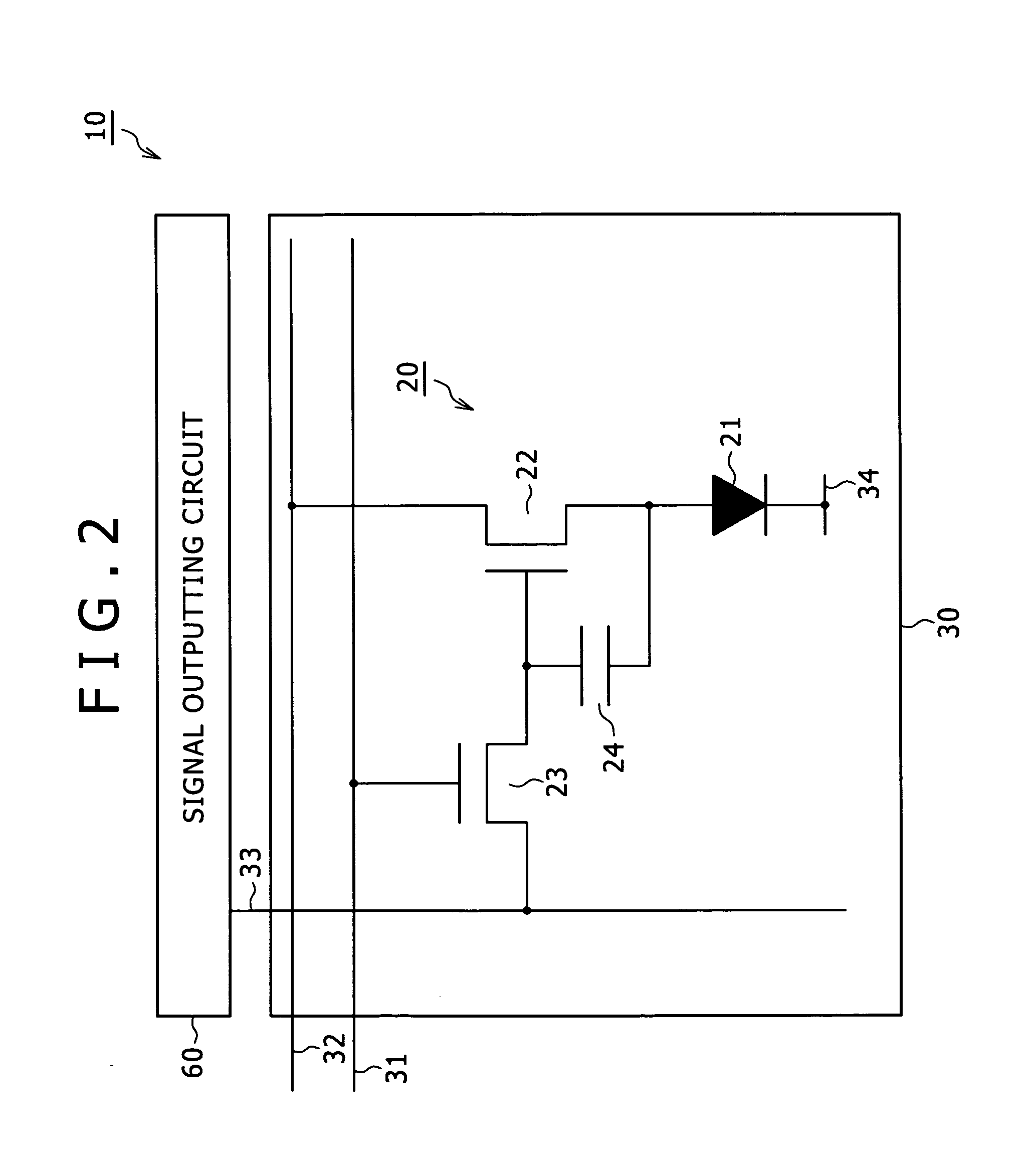
[0048]FIG. 1 is a block diagram showing a general system configuration of an active matrix display apparatus to which an embodiment of the present invention is applied. Here, it is assumed that the active matrix display apparatus described is an active matrix organic EL display apparatus wherein an organic EL element which is an electro-optical element of the current driven type whose emitted light luminance varies in response the value of current flowing through the element is used as a light emitting element of a pixel or pixel circuit.
[0049]Referring to FIG. 1, the organic EL display apparatus 10 shown includes a plurality of pixels 20 each including a light emitting element, a pixel array section 30 in which the pixels 20 are arranged two-dimensionally in rows and columns, that is, in a matrix, and driving sections disposed around the pixel array section 30. The driving sections drive the pixels 20 of the pixel array section 30 to emit light.
[005...
working example 1
1-1. Working Example 1
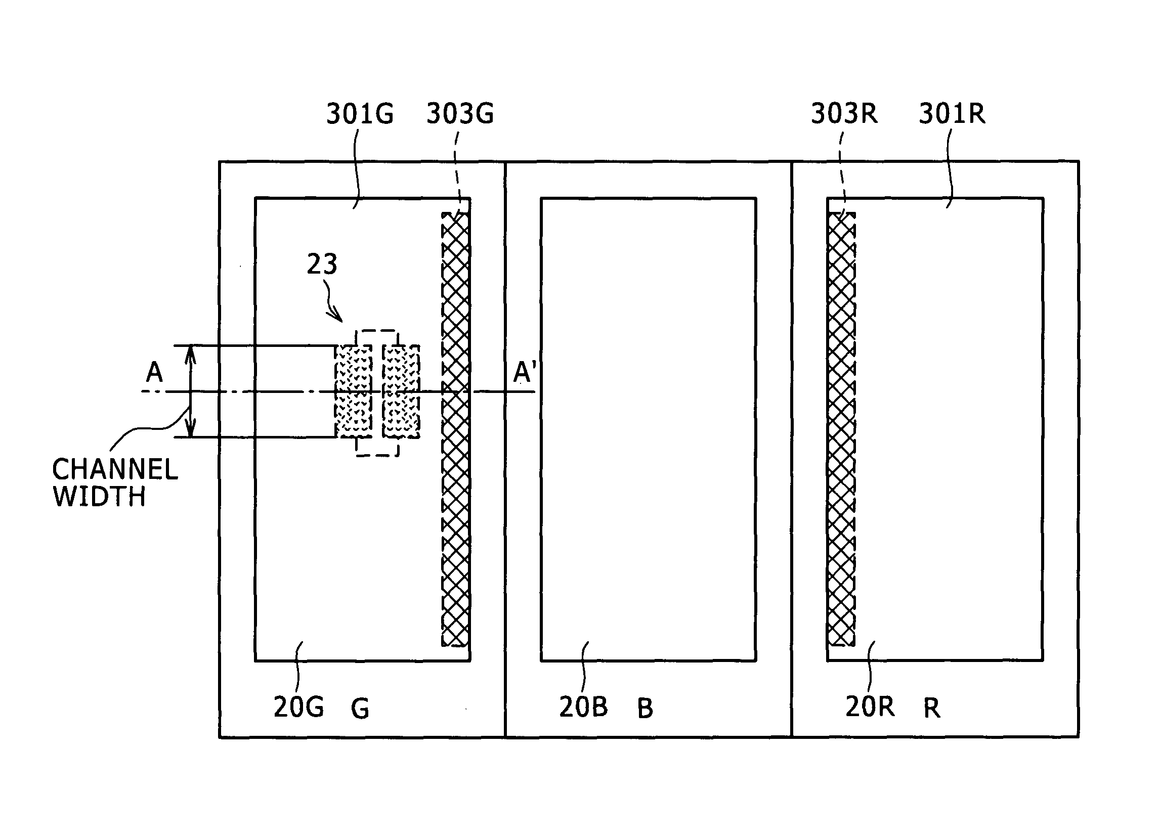
[0155]FIG. 14 is a plan view showing the light blocking layout structure according to a working example 1. Here, as an example, the light blocking layout structure exhibits a color array wherein R, G and B pixels or subpixels 20R, 20G and 20B are arranged such that the B pixel 20B is positioned centrally and the R and G pixels 20R and 20B are positioned on the opposite sides of the B pixel 20B. FIG. 15 shows a sectional structure of the light blocking layout structure taken along line A-A′ of FIG. 14.
[0156]Since the B pixel 20B is disposed centrally as seen in FIG. 14, transistors in the R and G pixels 20R and 20G positioned on the opposite sides of the B pixel 20B are influenced by irradiation of blue light emitted from the B pixel 20B. In order to prevent incidence of blue light from the B pixel 20B, a metal wiring layer 301G is provided in the layer same as that of the anode electrode of the G pixel 20G on the writing transistor 23, on the organic EL element...
modification 1
to the Working Example 1
[0160]FIG. 16 is a plan view showing a light blocking layout structure according to a modification 1 to the working example 1. In the light blocking layout structure according to the modification 1, light blocking members 303B-1 and 303B-2 having a width greater than the channel width of the writing transistor 23 are provided between R and G pixels 20R and 20B positioned adjacent to and on the opposite sides of the B pixel 20B.
[0161]With the light blocking layout structure according to the modification 1, blue light emitted from the B pixel 20B can be prevented from being reflected by the light blocking members 303G and 303R of the adjacent pixels and entering the B pixel 20B. Accordingly, not only with regard to the R and G pixels 20R and 20B but also with regard to the B pixel 20B, the characteristic shift by an influence of irradiation of blue light can be suppressed to a small amount.
PUM
 Abstract
Description
Claims
Application Information
 - R&D
- Intellectual Property
- Life Sciences
- Materials
- Tech Scout
- Unparalleled Data Quality
- Higher Quality Content
- 60% Fewer Hallucinations
Browse by: Latest US Patents, China's latest patents, Technical Efficacy Thesaurus, Application Domain, Technology Topic, Popular Technical Reports.
© 2025 PatSnap. All rights reserved.Legal|Privacy policy|Modern Slavery Act Transparency Statement|Sitemap|About US| Contact US: help@patsnap.com


