Semiconductor device integrated with converter and package structure thereof
a technology of semiconductor devices and converters, applied in semiconductor devices, semiconductor/solid-state device details, electrical apparatuses, etc., can solve problems such as power loss during voltage conversion, and achieve the effect of reducing the turn-on resistance and reducing the power loss during power supply conversion
- Summary
- Abstract
- Description
- Claims
- Application Information
AI Technical Summary
Benefits of technology
Problems solved by technology
Method used
Image
Examples
first embodiment
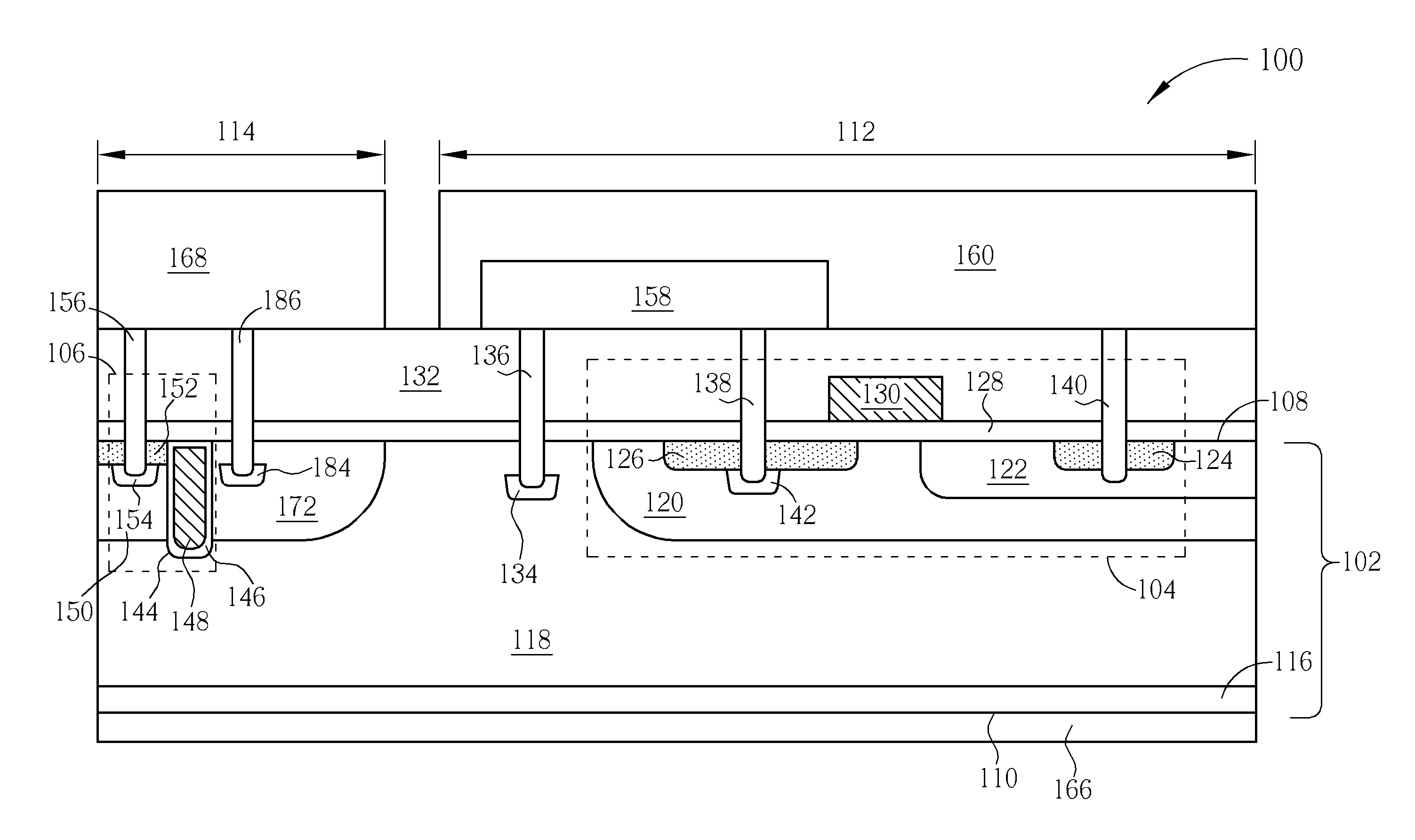
[0042]In addition, the N-type doped high-side source region of the present invention is not limited to be electrically connected to the N-type semiconductor substrate by means of the high-side source metal layer and the first contact plug. Please refer to FIG. 11. FIG. 11 is a cross-sectional view of a semiconductor device according to a second exemplary embodiment of the present invention. Same components are denoted by same numerals as the first exemplary embodiment in the following exemplary embodiments, and same structures are not redundantly detailed. As shown in FIG. 11, compared to the first exemplary embodiment, the semiconductor device 300 of this exemplary embodiment excludes the high-side source metal layer 162 and the first contact plug 136 used for electrically connecting the doped high-side source region 126 to the semiconductor substrate 102, and a second interlayer dielectric layer 302 of this exemplary embodiment totally covers a second contact plug 304 for electric...
first exemplary embodiment
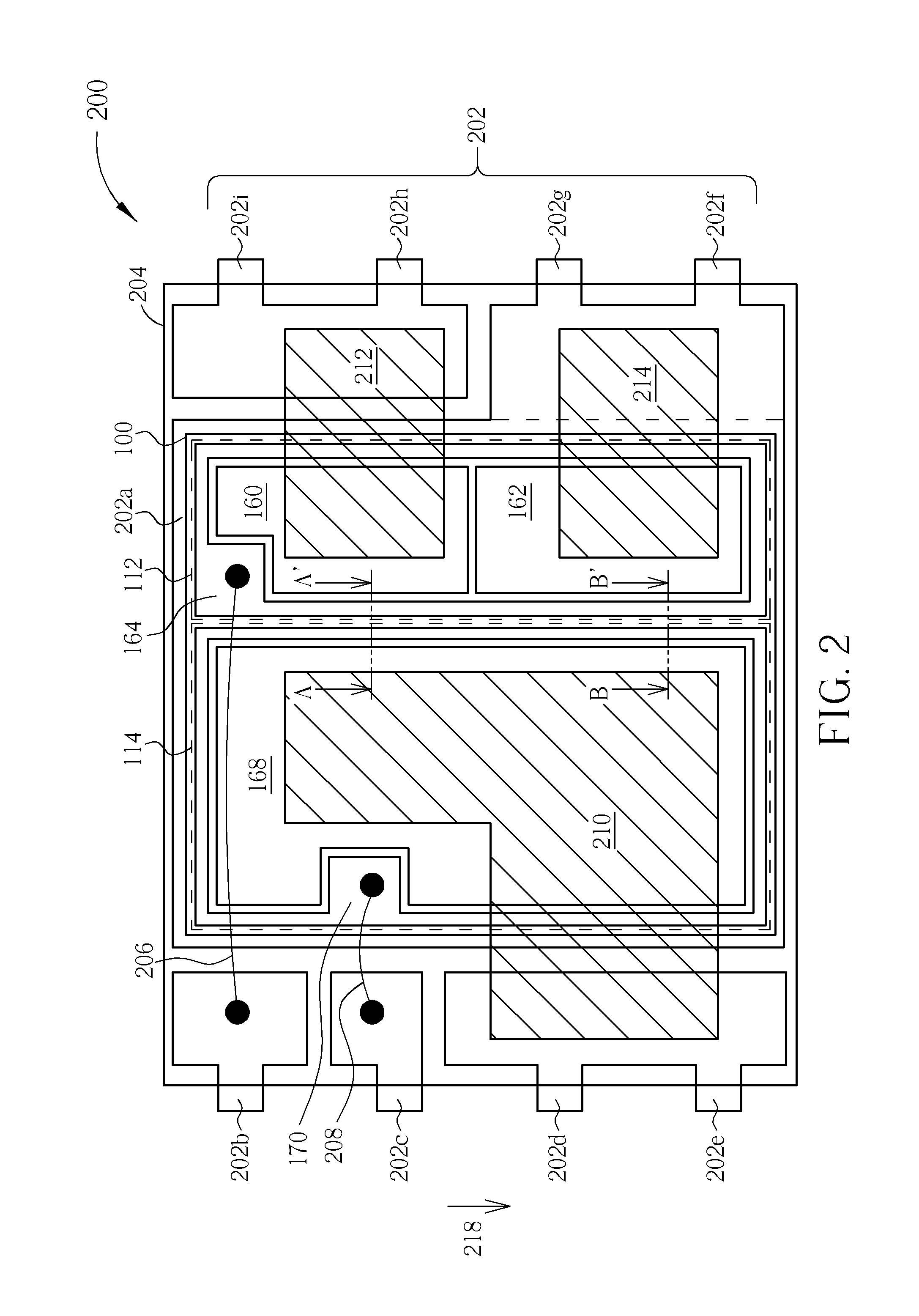
[0044]In addition, the structure of the lead frame is not limited to the structures of the previous exemplary embodiments. Please refer to FIG. 13. FIG. 13 is a top-view illustrating a package structure of a semiconductor device according to a third exemplary embodiment of the present invention. As shown in FIG. 13, compared to the first exemplary embodiment, the fifth lead 202f, the sixth lead 202g, the seventh lead 202h, and the eighth lead 202i in the package structure 450 of the semiconductor device 400 according to this exemplary embodiment are arranged along a direction reverse to the direction of the That is to say, the fifth lead 202f, the sixth lead 202g, the seventh lead 202h, and the eighth lead 202i are arranged along the first direction 218 in sequence, and the fifth lead 202f, the sixth lead 202g are still connected to the chip holder 202a. It is appreciated that, for electrically connecting the high-side source metal layer 162 to the common metal layer 166, the arran...
PUM
 Abstract
Description
Claims
Application Information
 - R&D
- Intellectual Property
- Life Sciences
- Materials
- Tech Scout
- Unparalleled Data Quality
- Higher Quality Content
- 60% Fewer Hallucinations
Browse by: Latest US Patents, China's latest patents, Technical Efficacy Thesaurus, Application Domain, Technology Topic, Popular Technical Reports.
© 2025 PatSnap. All rights reserved.Legal|Privacy policy|Modern Slavery Act Transparency Statement|Sitemap|About US| Contact US: help@patsnap.com


