
Active rectifying apparatus

a technology of active rectifying and rectifying device, which is applied in the direction of fixed transformer, analogue computer, electronic commutator, etc., can solve the problems of large power loss of diodes, which require forward voltages of, for example, 0.7 v, and achieve the effect of higher withstand voltage and higher withstand voltag

Active Publication Date: 2013-04-09
SOCIONEXT INC
View PDF5 Cites 4 Cited by
  • Summary
  • Abstract
  • Description
  • Claims
  • Application Information

AI Technical Summary

Problems solved by technology

A diode, which requires a forward voltage of, for example, 0.7 V, may have a large power loss.

Method used


Image

  • Active rectifying apparatus
  • Active rectifying apparatus
  • Active rectifying apparatus

Examples


Embodiment Construction

[0026]Power consumption may be reduced by detecting the voltage between the terminals of a diode and short-circuiting the terminals of the diode using a switch during forward conduction.

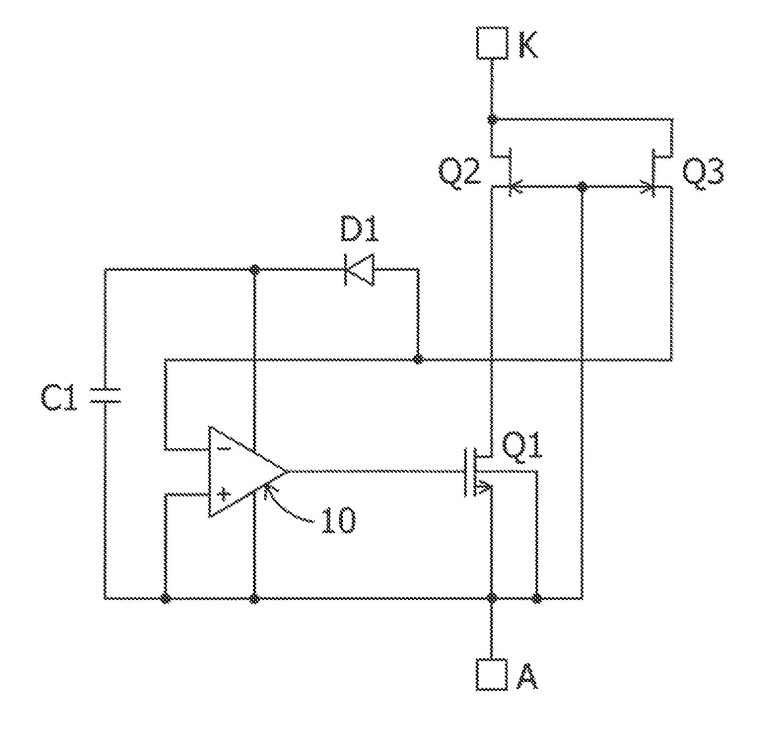
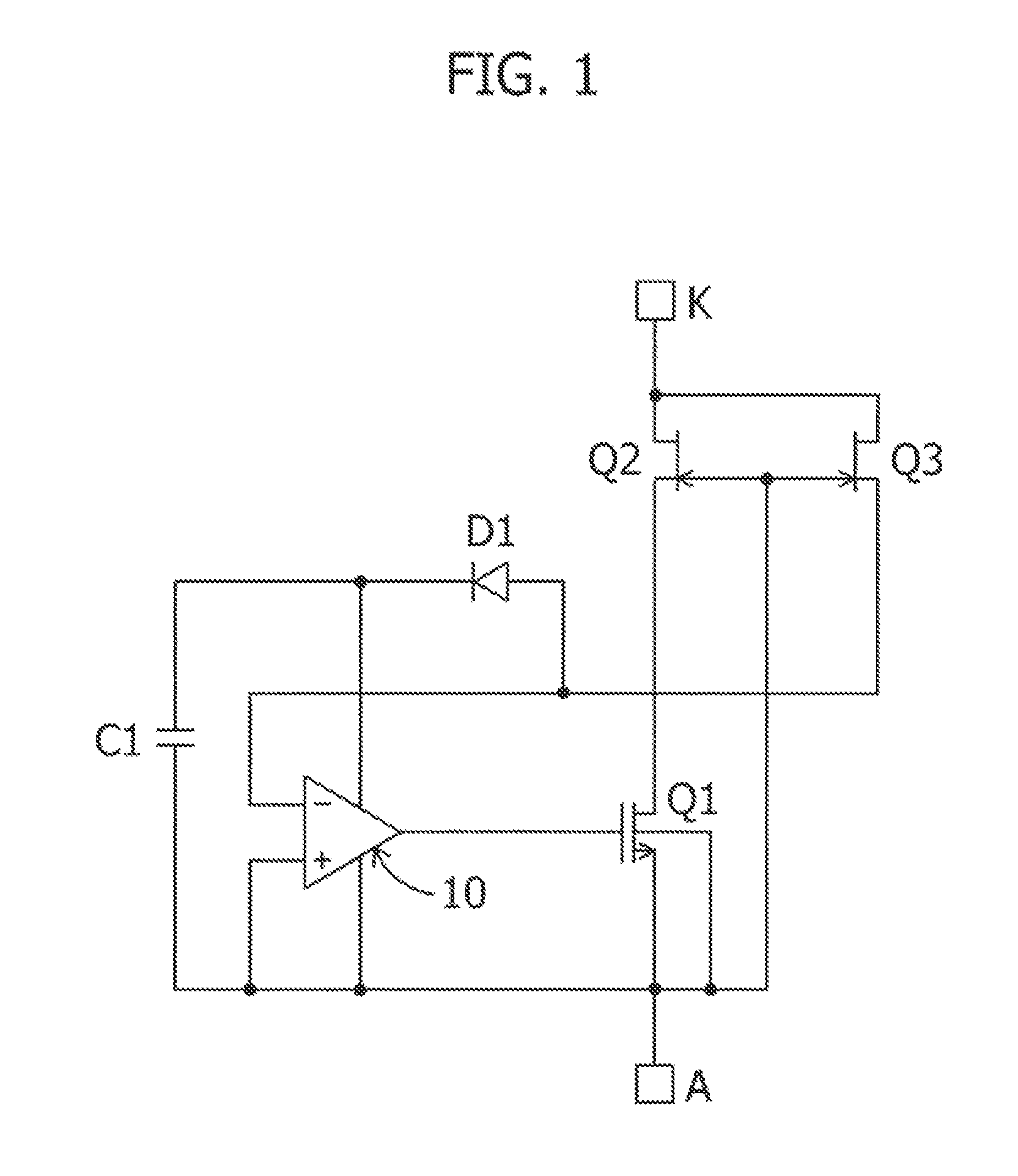
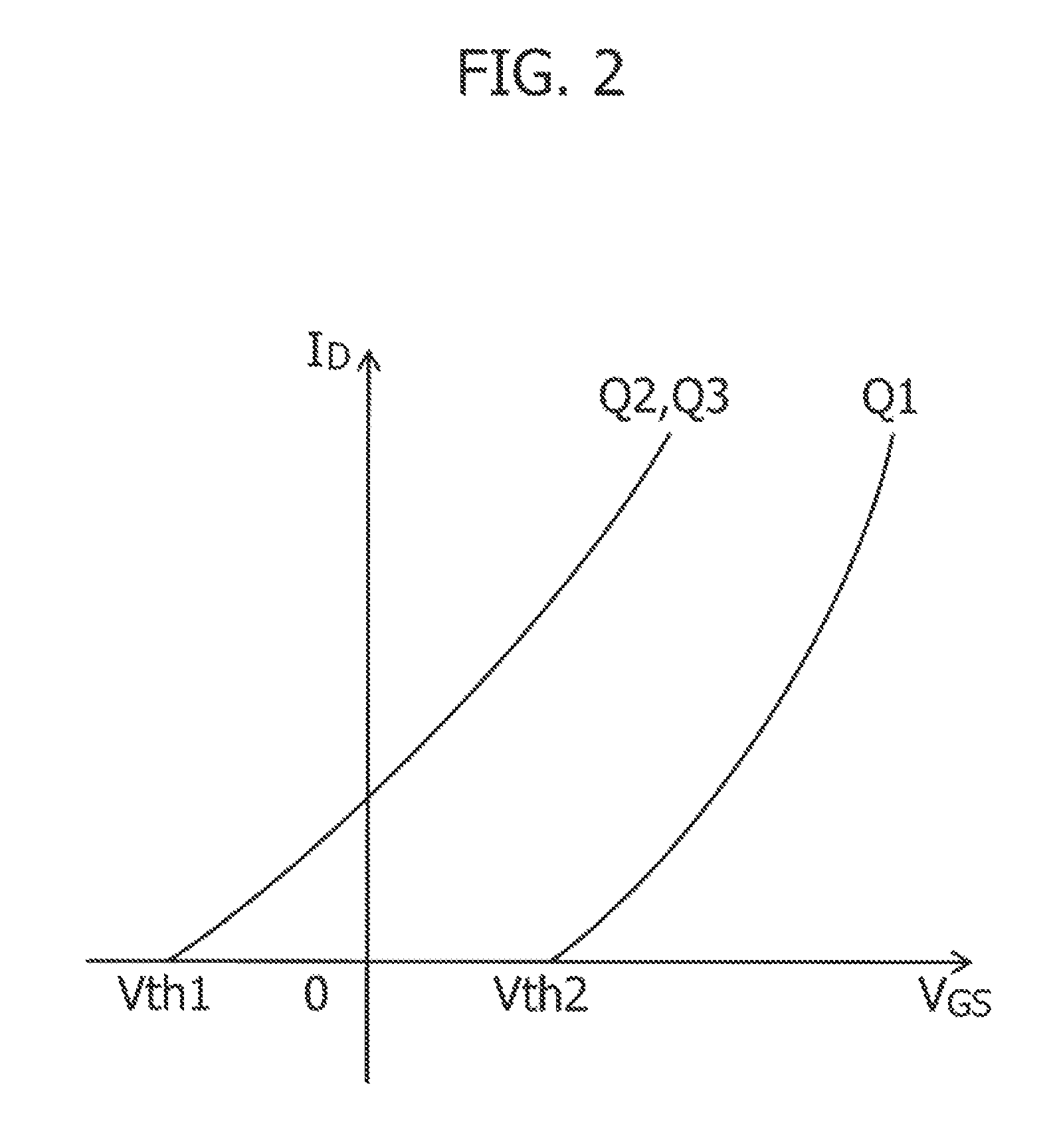
[0027]FIG. 1 illustrates an exemplary semiconductor apparatus. The semiconductor apparatus illustrated in FIG. 1 includes transistors Q1, Q2, and Q3, a comparator 10, a diode D1, and a capacitor C1. FIG. 2 illustrates exemplary characteristics of transistors. Referring to FIG. 2, the transistor Q1 may be a normally-off enhancement transistor, and the transistors Q2 and Q3 may be normally-on depletion mode transistors. The transistors Q2 and Q3 may be high-voltage (several hundreds to a thousand volts, for example) transistors, in comparison with the transistor Q1. For example, the transistor Q1 may by an n-channel silicon MOSFET, and the transistors Q2 and Q3 may be high electron mobility transistors (HEMTs) including a wide band gap semiconductor such as gallium nitride (GaN). The comparator 10 incl...


PUM


Abstract

A semiconductor apparatus includes: a first transistor; a second transistor having a higher withstand voltage than the first transistor, a source of the second transistor coupled to a drain of the first transistor, a gate of the second transistor coupled to a source of the first transistor; a third transistor having a higher withstand voltage than the first transistor and a drain of the third transistor coupled to a drain of the second transistor; and a comparator that compares a source voltage of the first transistor with a source voltage of the third transistor, and controls a gate voltage of the first transistor.

Description

CROSS-REFERENCE TO RELATED APPLICATIONS[0001]This application is a continuation-in-part of prior application Ser. No. 12 / 972,712, filed on Dec. 20, 2010, which has been abandoned. This application is based upon and claims the benefit of priority of the prior Japanese Patent Application No. 2009-290304 filed on Dec. 22, 2009, and the prior Japanese Patent Application No. 2010-271891, filed on Dec. 6, 2010, the entire contents of which are incorporated herein by reference.BACKGROUND[0002]1. Field[0003]The embodiments discussed herein relate to a semiconductor apparatus.[0004]2. Description of Related Art[0005]A rectifier device includes a diode in which a p-type semiconductor and a n-type semiconductor are joined. A diode, which requires a forward voltage of, for example, 0.7 V, may have a large power loss.[0006]A related technology is disclosed in, for example, Japanese Laid-open Patent Publication No. H7-297699.SUMMARY[0007]According to one aspect of the embodiments, a semiconductor...

Claims


Application Information

Patent Timeline
Patent Type & Authority Patents(United States)
IPC IPC(8): H03K17/74H03G11/02
CPCH03K17/302H01L27/0817H03K2017/307H01L27/088
Inventor TSUCHIYA, CHIKARA
Owner SOCIONEXT INC
Learn More