RFID tag located on metallic surfaces that have an increased communication range

a radio frequency identification and metallic surface technology, applied in the direction of resonant antennas, burglar alarm mechanical actuation, instruments, etc., can solve the problems of reducing the communication distance due to the change of the resonance point of the first antenna, and the rfid tag is likely to fall off the surface of the metal material, so as to reduce the influence of the polarization plane of the receiving antenna, reduce the change in the communication distance, and reduce the effect of the change of the resonance poin

Inactive Publication Date: 2013-04-02
HITACHI LTD
View PDF19 Cites 6 Cited by
  • Summary
  • Abstract
  • Description
  • Claims
  • Application Information

AI Technical Summary

Benefits of technology

[0004]However, while a desired communication distance can be attained by placing an insulator or a soft magnetic material having a predetermined thickness (for example a thickness of 1 mm or more) between the tag antenna and the attaching surface of a metal material, the entire RFID tag becomes thicker, which makes the RFID tag likely to fall off the surface of the metal material. Furthermore, in the case of the technique disclosed in the related art given above, the resonance point of the tag antenna can vary depending on whether the RFID tag is attached to the surface of an object made of a metal material or an object made of a nonmetal material due to the layered structure of the tag antenna and the soft magnetic material. That is, since changes in the electric potential on a metal surface are small, the electric potential distribution of the tag antenna can change and therefore the resonance point can change. When the RFID tag is attached to a nonmetal object with a soft magnetic material between them, a change of the resonance point of the tag antenna (first tag antenna) can reduce the communication distance.
[0005]The present invention has been made in light of the problems described above and an object of the present invention is to provide an RFID tag capable of reducing variations in communication distance even when the resonance point of a first antenna changes.
[0007]With this RFID tag, since the second antenna connected to one end of the first antenna has an electrical length of an integral multiple of λ / 2, the second antenna resonates through the first antenna regardless of the length of the first antenna. Consequently, variations in the communication distance due to changes of the resonance point of the first antenna are reduced. In particular, the influence of the plane of polarization of a receiving antenna is reduced when the first and second antennas are electrically connected or electrostatically coupled with each other at an angle of approximately 90 degrees, because the planes of polarization of electromagnetic waves emitted from the first and second antennas are approximately orthogonal to each other. This also reduces changes in the communication distance. In particular, even if the surface of a metal is close to the tag antenna with a spacer between them, a desired communication distance can be achieved. Changes in resonance frequency are small even when the RFID tag is attached to a metal material with a spacer made from a resin film, rather than a soft magnetic material, disposed on the back side.
[0008]In the RFID tag according to the present invention, the second antenna resonates through the first antenna. Therefore, variations in the communication distance can be reduced even when the resonance point of the first antenna changes. In particular, variations in the communication distance can be reduced even when the back side of the RFID tag is attached to the surface of a metal.

Problems solved by technology

However, while a desired communication distance can be attained by placing an insulator or a soft magnetic material having a predetermined thickness (for example a thickness of 1 mm or more) between the tag antenna and the attaching surface of a metal material, the entire RFID tag becomes thicker, which makes the RFID tag likely to fall off the surface of the metal material.

Method used


Image

  • RFID tag located on metallic surfaces that have an increased communication range
  • RFID tag located on metallic surfaces that have an increased communication range
  • RFID tag located on metallic surfaces that have an increased communication range

Examples


first embodiment

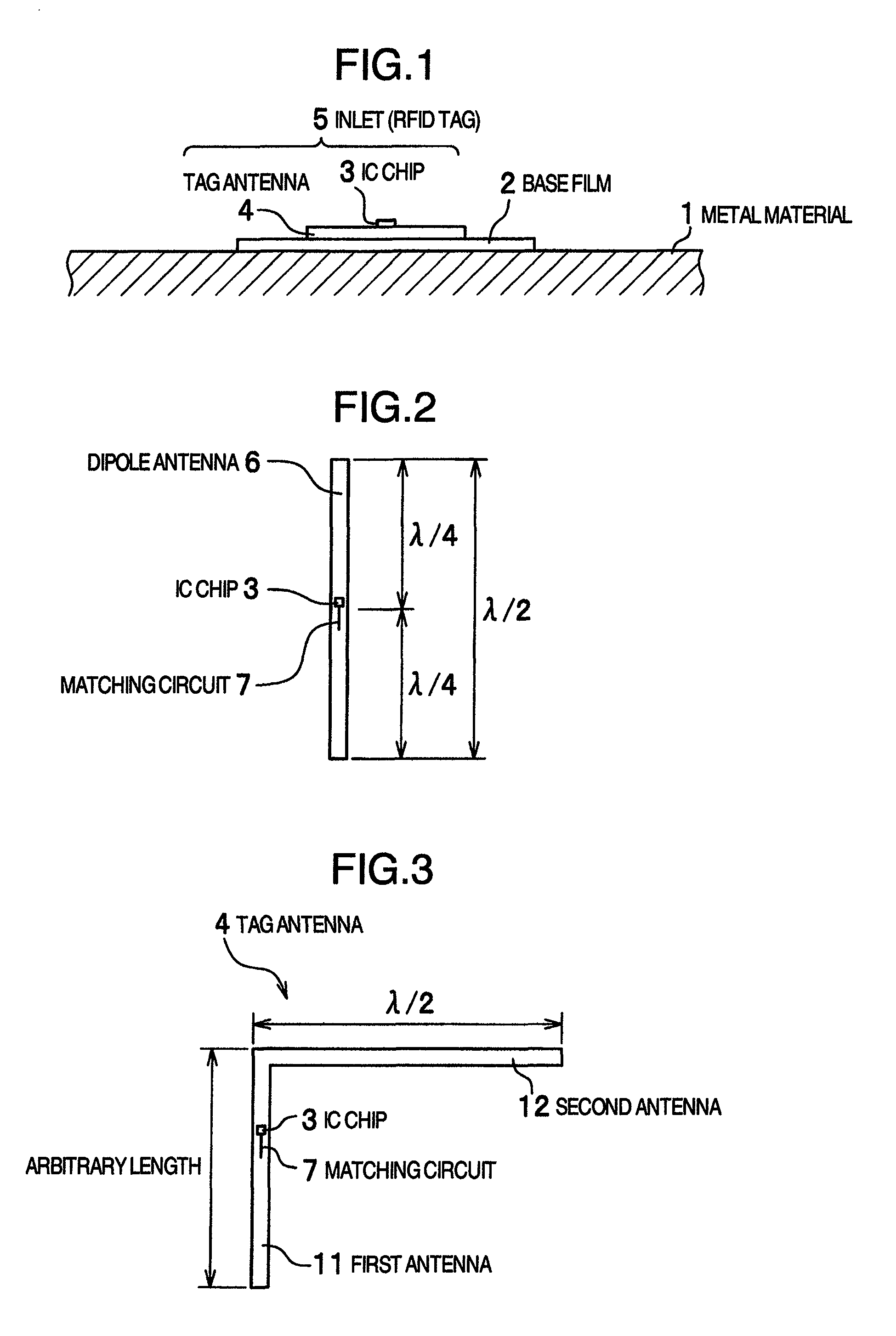
[0035]Embodiments of an RFID tag according to the present invention will be described below in detail with reference to the accompanying drawings. FIG. 1 is a cross-sectional view of an RFID tag attached to a surface of a metal material. A tag antenna 4 having an IC chip 3 mounted thereon (hereinafter an arrangement including the IC chip 3 and the tag antenna 4 is referred to as an inlet 5 and an arrangement laminated with an outer film or films, not shown, is referred to as an RFID tag) is attached to a surface of a resin base film 2 by an adhesive or the like. The base film 2, which acts as a spacer, is placed between the surface of a metal material 1 and the tag antenna 4. Thus, information recorded on the IC chip 3 can be read and written by a reader / writer (not shown) when the reader / writer is passed near the tag antenna 4.

[0036]FIG. 2 is a top view showing an RFID tag that uses a dipole antenna as the tag antenna 4 shown in FIG. 1. The dipole antenna 6 has an electrical length...

second embodiment

[0062]Several variations of the strip tag antenna have been described in the first embodiment. Several variations of a wide tag antenna having a wide second antenna will be described in a second embodiment.

First Variation of Wide Tag Antenna

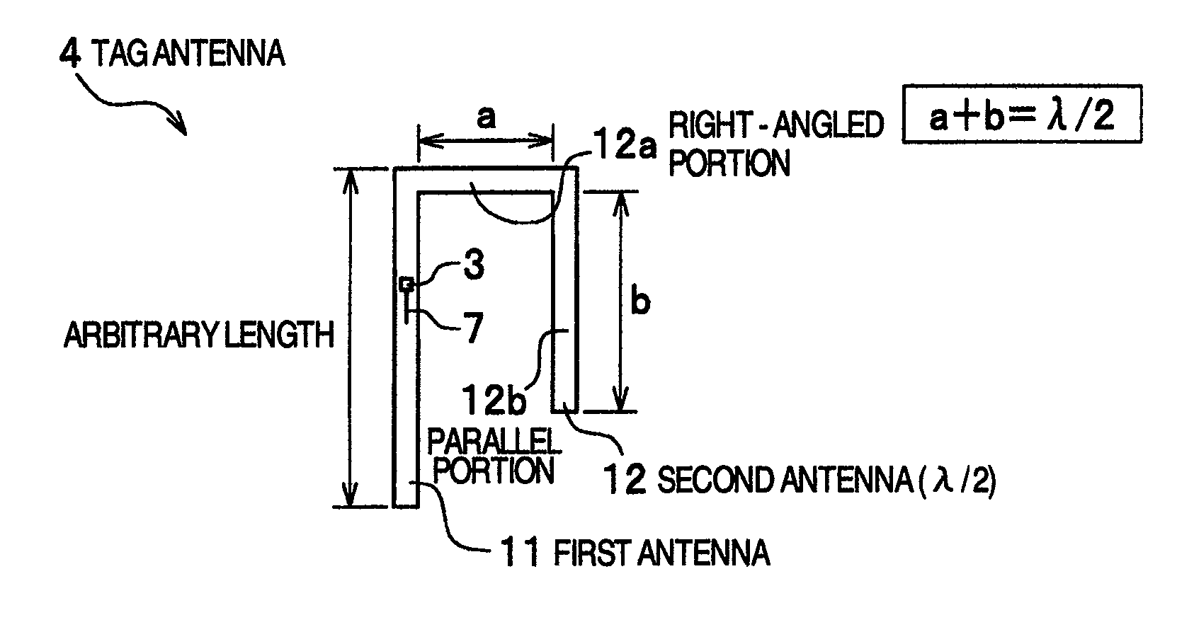
[0063]FIG. 12 is a configuration diagram of a first variation of a wide tag antenna according to the second embodiment. In this variation, the configuration of the first variation of the first embodiment shown in FIG. 3 is modified to increase the width of the second antenna. That is, as shown in FIG. 12, a longer side of a rectangular second antenna 22 wider than a first antenna 21 having an IC chip 3 mounted thereon is connected to an end of the first antenna 21. The second antenna 22 extends in a direction at right angles to the first antenna 21. The first antenna 21 has an arbitrary length. The wide second antenna 22 extending from the end of the first antenna 21 at right angles has an electrical length of λ / 2 or λ / 2 multiplied by n (where n ...

third embodiment

[0072]In a third embodiment, a detailed description will be given of an embodiment in which a tag antenna is formed on a base film, an embodiment in which a first antenna is electrically coupled with a second antenna, and an embodiment in which an inlet formed by a tag antenna on which an IC chip is mounted is laminated with a protective film to form an RFID tag.

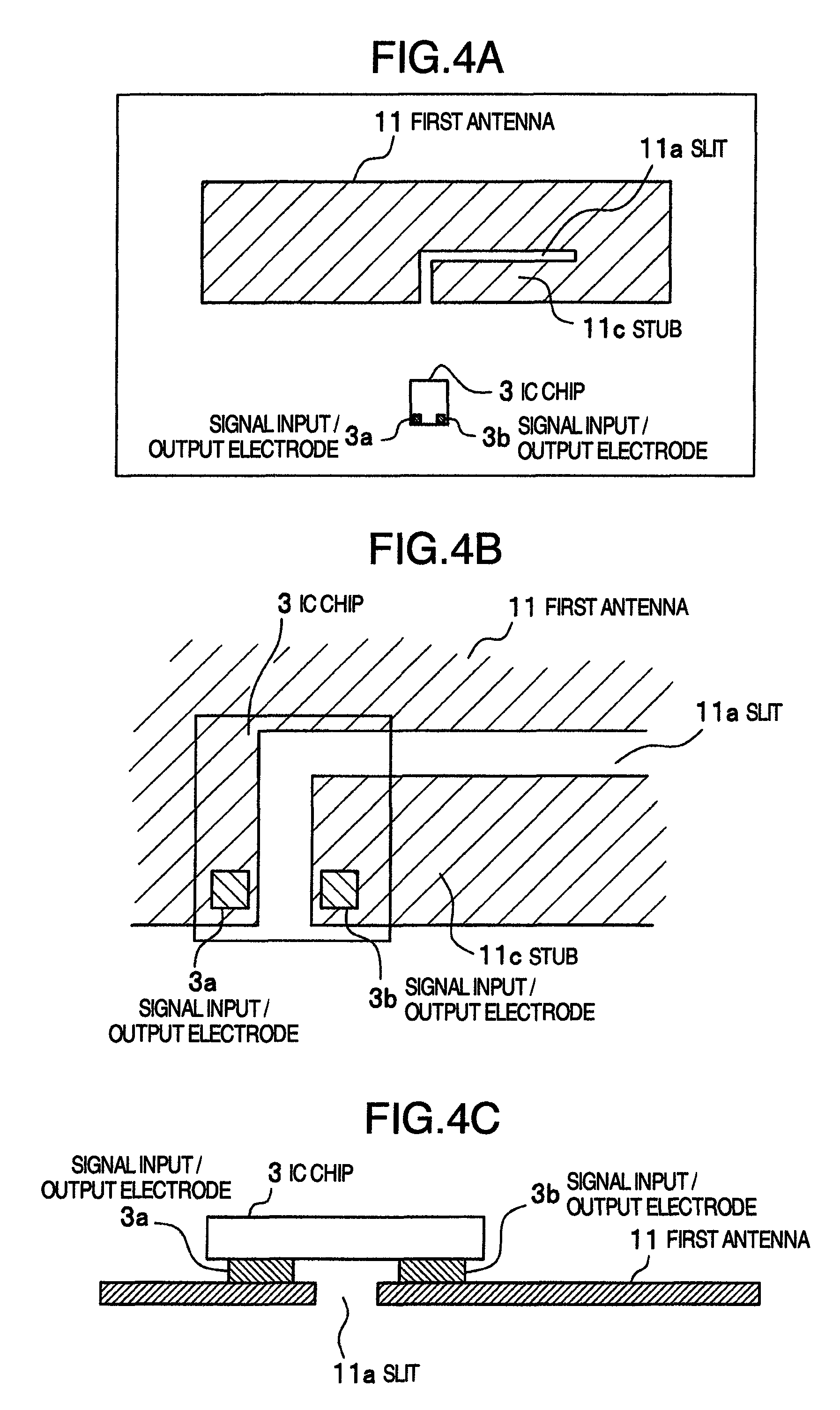
[0073]FIG. 18 is a conceptual diagram of one embodiment, viewed from above, in which a tag antenna is formed on a base film according to the third embodiment. First and second antennas 21 and 22 each having a thickness of on the order of several tens of μm are contiguously deposited by metal vapor deposition or formed of a metal foil on a base film 2 made of a heat-resistant polyimide film having a thickness of approximately 30 μm, for example. Then, a slit is formed in a predetermined position on the first antenna 21, a matching circuit 7 is provided, and an IC chip 3 is mounted on it. A tag antenna 4 is thus formed, where ...


PUM


Abstract

An RFID tag includes a first antenna on which an IC chip is mounted and a second antenna extending from an end of the first antenna in a direction at right angles to the first antenna. The first antenna has an arbitrarily electrical length and the second antenna has an electrical length of λ / 2 or an integral multiple of λ / 2. A resin base film having a thickness of approximately 50 μm is disposed on the back side of the first antenna and the second antenna. With this configuration of a tag antenna, the second antenna resonates with the first antenna to exhibit a radio wave amplifying effect. Therefore, a long communication distance can be achieved even if the electrical length of the first antenna is chosen to be short or the thickness of the base film is chosen to be thin.

Description

INCORPORATION BY REFERENCE[0001]The present application claims priority from Japanese application JP2007-103791 filed on Apr. 11, 2007, the content of which is hereby incorporated by reference into this application.BACKGROUND OF THE INVENTION[0002]The present invention relates to an RFID (Radio Frequency Identification) tag that transmits information such as ID (Identification) information recorded on an IC chip at an RF (Radio Frequency).[0003]An RFID tag consists of an IC chip and a tag antenna and is capable of transmitting information such as ID recorded on the IC chip through the tag antenna via a radio frequency (RF). Accordingly, by passing the RFID tag near a reader / writer, information recorded on the IC chip can be read in a noncontact manner at a relatively long communication distance (for example approximately 140 mm). Therefore, RFID tags are often used for production management and logistics management of products fabricated at factories. However, the communication dist...

Claims


Application Information

Patent Timeline
Patent Type & Authority Patents(United States)
IPC IPC(8): G08B13/14
CPCG06K19/07749G06K19/07767H01Q1/2225H01Q9/065H01Q1/2283
Inventor SAKAMA, ISAO
Owner HITACHI LTD
Why Eureka
Try Eureka