Pixel and organic light emitting display device using the same

a technology of light-emitting display device and pixel, which is applied in semiconductor devices, instruments, computing, etc., can solve the problems of six transistors included in the pixel, the inability to display an image with uniform luminance, and the inability to simplify the pixel b>4/b>, so as to reduce or minimize the number of transistors included.

Active Publication Date: 2013-03-19
SAMSUNG DISPLAY CO LTD
View PDF11 Cites 4 Cited by
  • Summary
  • Abstract
  • Description
  • Claims
  • Application Information

AI Technical Summary

Benefits of technology

[0015]Accordingly, an aspect of the present invention provides a pixel having a simple structure and configured to compensate for the threshold voltage of a driving transistor, and an organic light emitting display device using the pixel.
[0030]According to one embodiment of the present invention, a pixel and an organic light emitting display device using the pixel, may compensate for a threshold voltage of a driving transistor while reducing or minimizing the number of transistors included in the pixel.

Problems solved by technology

However, the pixel 4 of the organic light emitting display device of the related art cannot display an image with uniform luminance.
However, the six transistors included in the pixel 4 complicate the pixel 4.

Method used


Image

  • Pixel and organic light emitting display device using the same
  • Pixel and organic light emitting display device using the same
  • Pixel and organic light emitting display device using the same

Examples


Embodiment Construction

[0037]Hereinafter, certain exemplary embodiments according to the present invention will be described with reference to the accompanying drawings. Here, when a first element is described as being coupled to a second element, the first element may be directly coupled to the second element or may be indirectly coupled to the second element via a third element. Further, some of the elements that are not essential to complete understanding of the invention are omitted for clarity. Also, like reference numerals refer to like elements throughout.

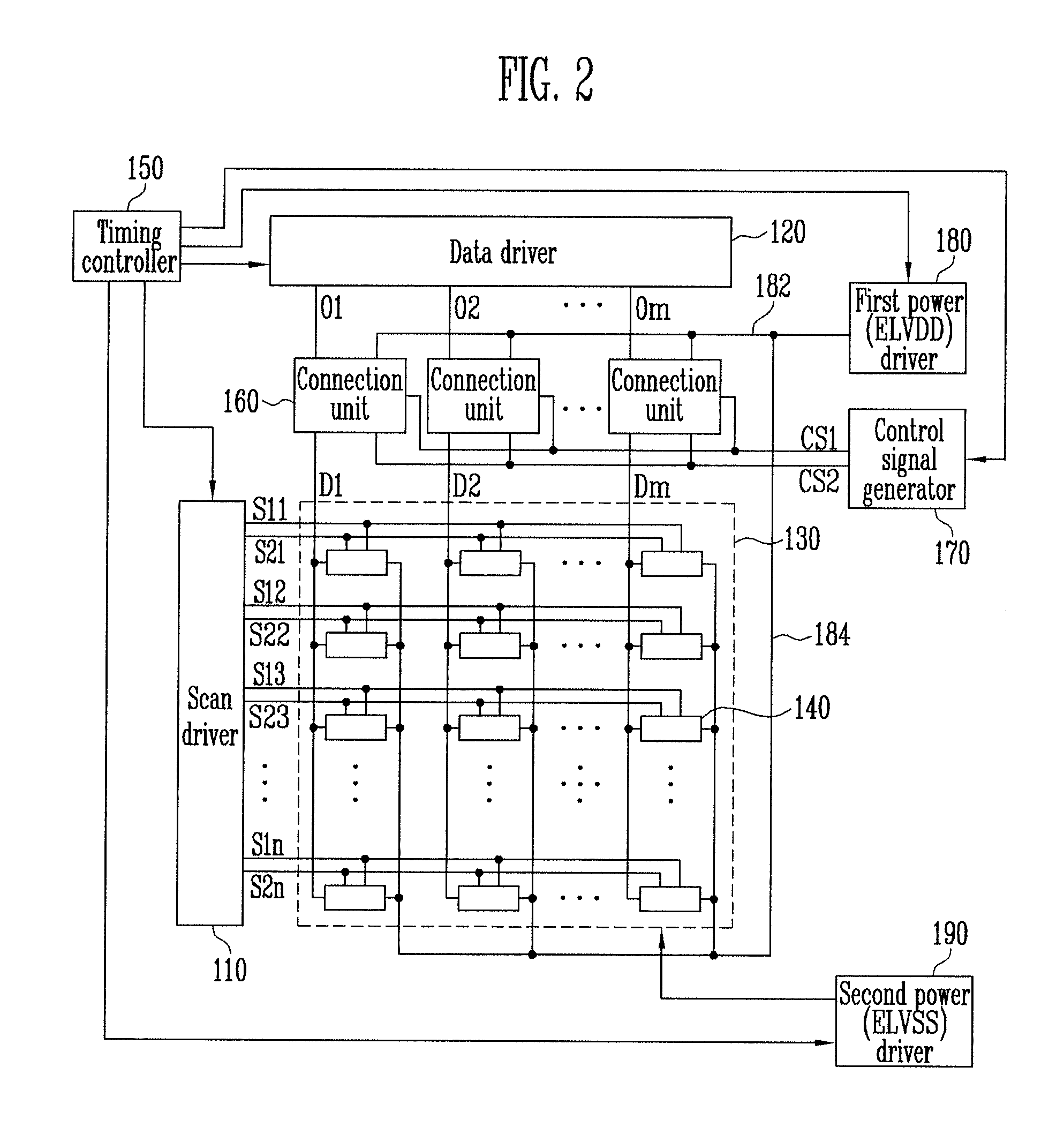
[0038]FIG. 2 is a block diagram illustrating an organic light emitting display device according to an embodiment of the present invention.

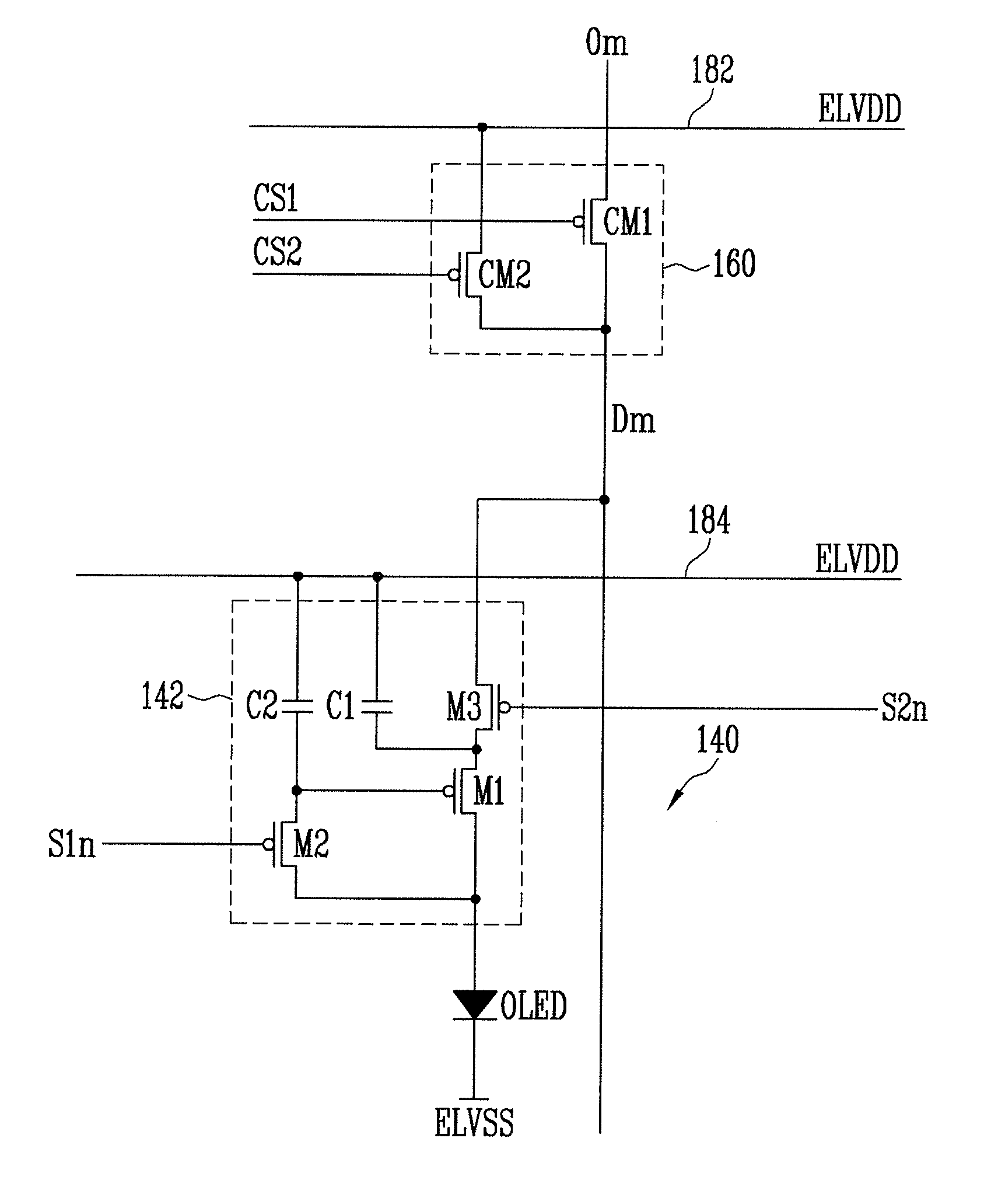
[0039]Referring to FIG. 2, an organic light emitting display device according to an embodiment of the present invention includes a display unit 130 including pixels 140 coupled with first scan lines S11 to S1n, second scan lines S21 to S2n, and data lines D1 to Dm, a scan driver 110 driving the first scan lines ...


PUM


Abstract

A pixel includes: an organic light emitting diode; a first transistor having a second electrode coupled with the organic light emitting diode and a first electrode coupled with a data line; a second transistor coupled between a gate electrode and the second electrode of the first transistor and turned on when a first scan signal is supplied to a first scan line; a third transistor coupled between the first electrode of the first transistor and the data line and turned on when a second scan signal is supplied to the second scan line; a first capacitor coupled between the first electrode of the first transistor and a first power supply; and a second capacitor coupled between the gate electrode of the first transistor and the first power supply.

Description

CROSS-REFERENCE TO RELATED APPLICATIONS[0001]This application claims priority to and the benefit of Korean Patent Application No. 10-2010-0069940, filed on Jul. 20, 2010, in the Korean Intellectual Property Office, the entire content of which is incorporated herein by reference.BACKGROUND[0002]1. Field of the Invention[0003]Aspects of embodiments according to the present invention relate to a pixel and an organic light emitting display device using the pixel, and an organic light emitting display device using the pixel.[0004]2. Description of Related Art[0005]A variety of flat panel displays which are lighter and smaller than cathode ray tubes have been recently developed. Various flat panel displays include liquid crystal displays (LCDs), field emission displays (FEDs), plasma display panels (PDPs), and an organic light emitting display devices, etc.[0006]The organic light emitting display device displays an image, using an organic light emitting diode that produces light by recomb...

Claims


Application Information

Patent Timeline
Patent Type & Authority Patents(United States)
IPC IPC(8): G09G3/30
CPCG09G3/3233G09G2300/0465G09G2300/0861G09G2300/0852G09G2300/0819
Inventor HWANG, YOUNG-IN
Owner SAMSUNG DISPLAY CO LTD
Why Eureka
Try Eureka