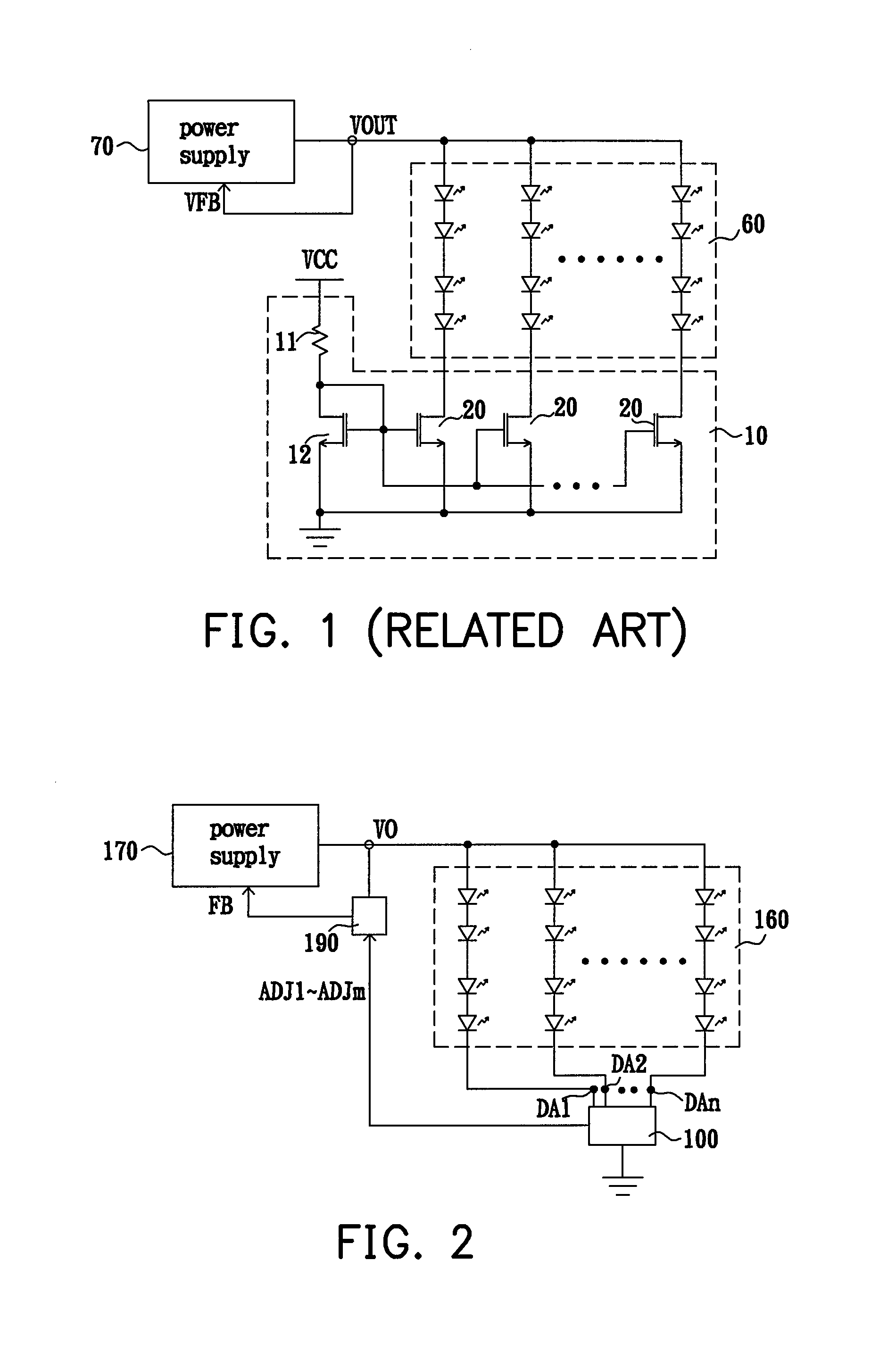
LED current control circuit, current balancer and driving apparatus
a current control circuit and current balance technology, applied in the direction of electric variable regulation, process and machine control, instruments, etc., can solve the problems of low achieve enhanced driving apparatus efficiency, reduce the efficiency of led current driving apparatus, and increase the driving voltage
- Summary
- Abstract
- Description
- Claims
- Application Information
AI Technical Summary
Benefits of technology
Problems solved by technology
Method used
Image
Examples
first embodiment
[0043]FIG. 7A is a schematic circuit diagram of a voltage feedback circuit according to the invention. Referring to FIG. 7A, in the present embodiment, the voltage feedback circuit includes a first resistor R1 and a second resistor R2. Herein, the second resistor R2 is an adjustable resistor. The adjustment determining circuit 230 adjusts the resistance of the second resistor R2 by controlling the level of the adjustment control signal ADJ. Accordingly, if any of the levels of the current balance ends DA1-DAn is lower than the voltage protecting value Vr, the adjustment determining circuit 230 decreases the resistance of the second resistor R2 to decrease the dividing ratio of the voltage feedback circuit. Hence, the power supply 170 increases the output voltage VO to increase the voltages of the current balance ends DA1-DAn. Furthermore, because of the characteristic of LED having the threshold voltage with a negative temperature parameter, when the temperature increases, the thres...
second embodiment
[0044]FIG. 7B is a schematic circuit diagram of a voltage feedback circuit according to the invention. Referring to FIG. 7B, in the present embodiment, the voltage feedback circuit includes a first resistor R1, a third resistor R3, and a plurality of adjusted resistors RA1-Ram connects in parallel with the third resistor R3. The adjusted resistors RA1-Ram are respectively coupled to the adjustment switches SW1-SWm in series, and the adjustment switches SW1-SWm are controlled by the adjustment control signals ADJ1-ADJm. When all of the adjustment switches SW1-SWm are cut off, the voltage feedback circuit stays in a first feedback mode. At this time, the voltage feedback circuit has a first dividing ratio R3 / (R1+R3), and the first dividing ratio corresponds to a first voltage value to have the output voltage VO being stabilized at the first voltage value. When the adjustment switch SW1 is turned on, and the adjustment switches SW2-SWm are cut off, the voltage feedback circuit stays in...
third embodiment
[0045]FIG. 7C is a schematic circuit diagram of a voltage feedback circuit according to the invention. Referring to FIG. 7C, in the present embodiment, the voltage feedback circuit includes a first resistor R1, a third resistor R3, a fourth resistor R4, and an adjustment circuit 295. The adjustment circuit 295 receives the adjustment control signals ADJ1-ADJm to correspondingly generate one of adjustment voltages V1-Vm. Herein, the adjustment voltages V1-Vm are gradually increased from the adjustment voltage V1 to the adjustment voltage Vm, i.e. the adjustment voltage V1 is smallest, and the adjustment voltage Vm is largest. The adjustment voltages V1-Vm adjust the level of the voltage feedback signal FB by the fourth resistor R4 and the dividing voltage of the third resistor R3. The predetermined initial voltage provided by the adjustment circuit 295 may be the adjustment voltage Vm. At this time, the voltage value at which the output voltage VO is stabilized is smallest. Next, acc...
PUM
 Abstract
Description
Claims
Application Information
 - R&D
- Intellectual Property
- Life Sciences
- Materials
- Tech Scout
- Unparalleled Data Quality
- Higher Quality Content
- 60% Fewer Hallucinations
Browse by: Latest US Patents, China's latest patents, Technical Efficacy Thesaurus, Application Domain, Technology Topic, Popular Technical Reports.
© 2025 PatSnap. All rights reserved.Legal|Privacy policy|Modern Slavery Act Transparency Statement|Sitemap|About US| Contact US: help@patsnap.com


