
Double side cooled power module with power overlay

a power module and power overlay technology, applied in electrical apparatus, semiconductor devices, semiconductor/solid-state device details, etc., can solve the problems of increasing the difficulty of cooling power semiconductor devices, natural and forced air cooling schemes cannot handle heat flux only, and manufacturing difficulties

Active Publication Date: 2013-01-22
GENERAL ELECTRIC CO
View PDF7 Cites 44 Cited by
  • Summary
  • Abstract
  • Description
  • Claims
  • Application Information

AI Technical Summary

Benefits of technology

The solution provides efficient thermal management with improved heat flux handling and reduced manufacturing complexity, achieving uniform temperature distribution without compromising cooling channel features.

Problems solved by technology

The development of higher-density power electronics has made it increasingly more difficult to cool power semiconductor devices.
When device temperatures are limited to 50 K increases, natural and forced air cooling schemes can only handle heat fluxes up to about one (1) W / cm2.
Heat pipes, impingement sprays, and liquid boiling are capable of larger heat fluxes, but these techniques can lead to manufacturing difficulties and high cost.
An additional problem encountered in conventional cooling of high heat flux power devices is non-uniform temperature distribution across the heated surface.
This is due to the non-uniform cooling channel structure, as well as the temperature rise of the cooling fluid as it flows through long channels parallel to the heated surface.
Further, these known micro-channel designs employ very complicated backside micro-channel structures and heat sinks that are extremely complicated to build and therefore very costly to manufacture.
Although power overlay technology (POL) has been employed to provide double-sided cooling, these known structures have not utilized micro-channel features to enhance thermal performance of POL modules.

Method used


Image

  • Double side cooled power module with power overlay
  • Double side cooled power module with power overlay
  • Double side cooled power module with power overlay

Examples


Embodiment Construction

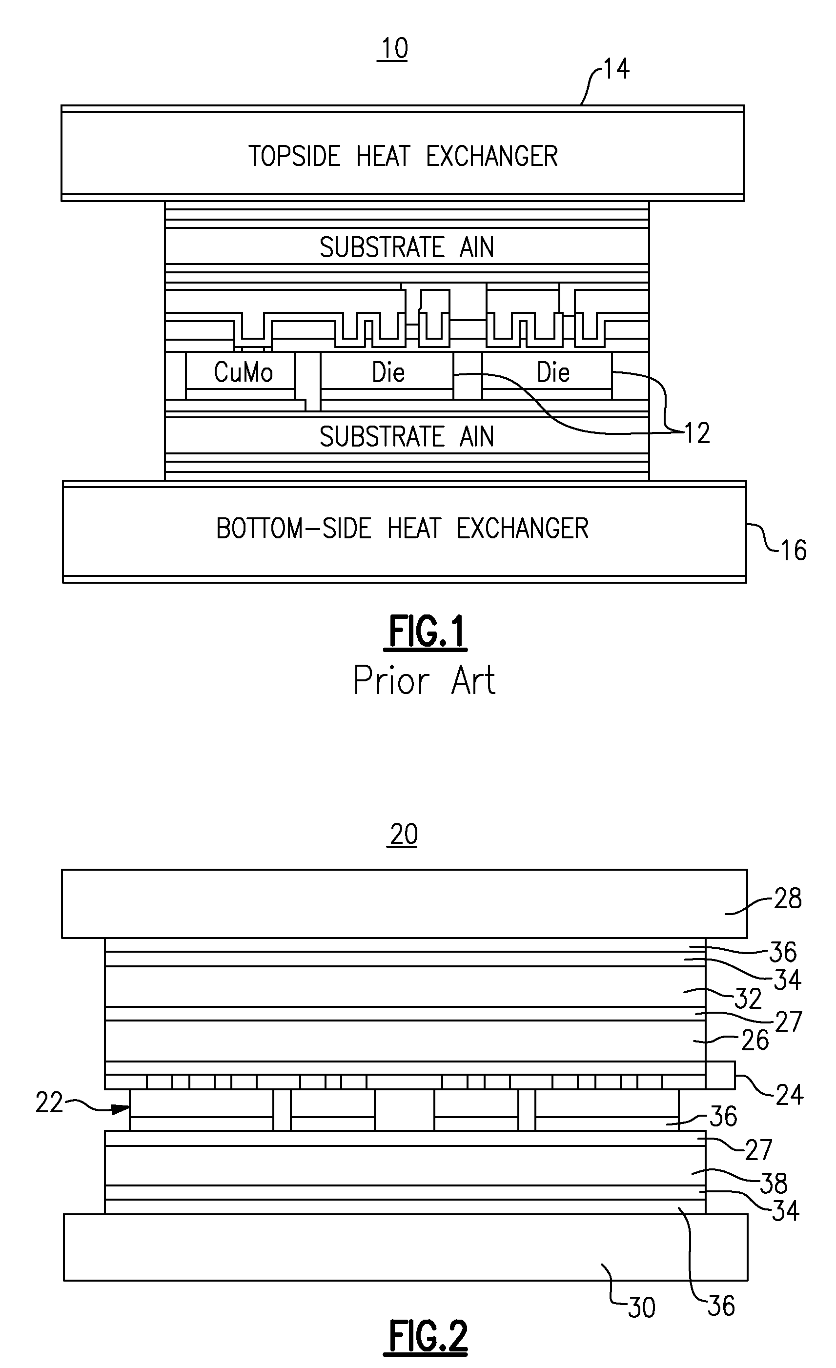
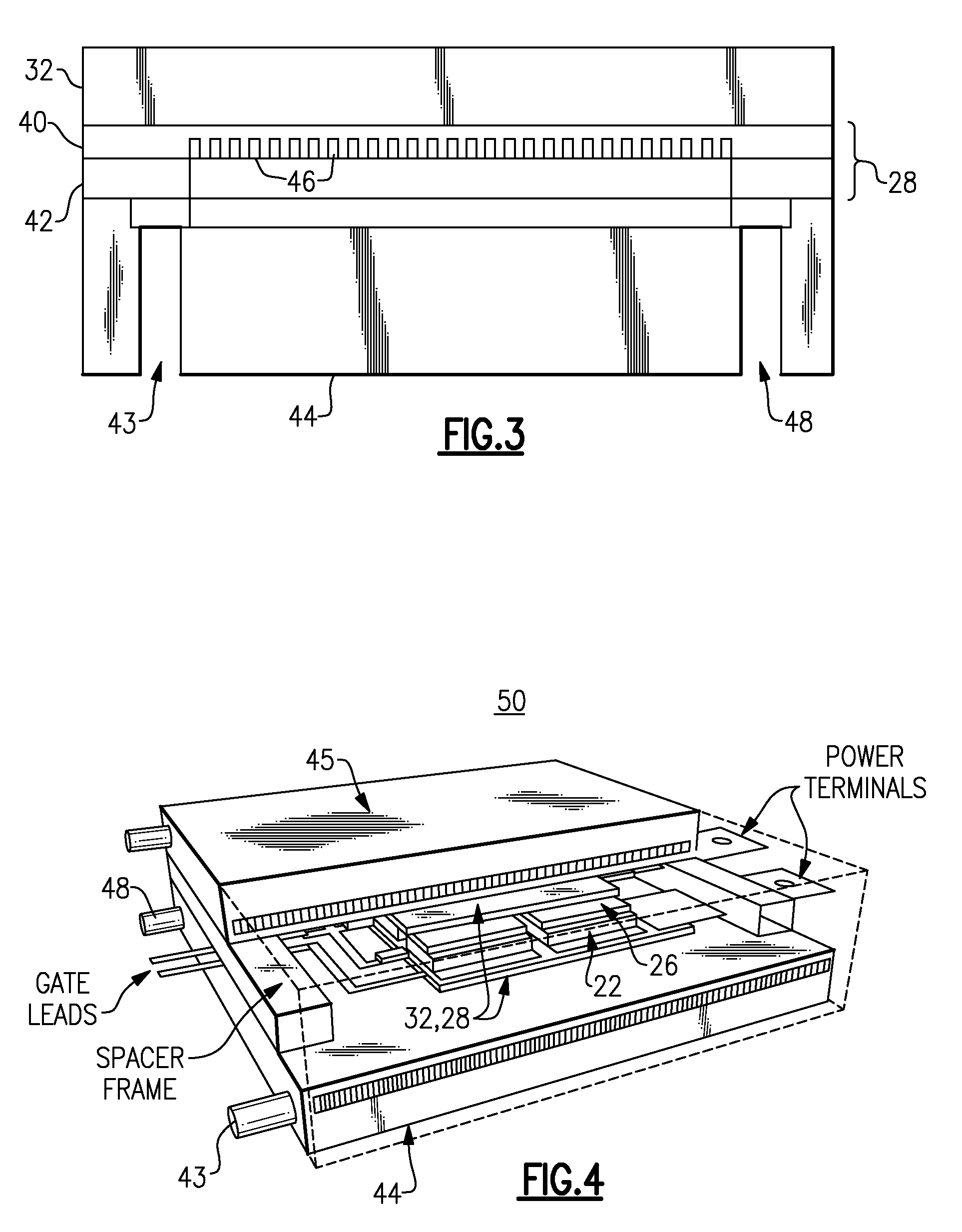
[0032]FIG. 1 is a side profile view illustrating a double side heat exchanger cooled power module 10 using power overlay technology that is known in the art. Double side cooling of semiconductor power modules using power overlay technology is known in the art. Because of the unique planar structure of the power overlay technology, modules using power overlay technology can be cooled from both the top and bottom sides of the power module since the elimination of wire bonds or even solder bumps from the top surface of the power devices subsequent to a smoothing operation leaves the top surface virtually planar. The structure illustrated in FIG. 1 can have a significantly lower junction temperature because the thermal cooling structure is connected to the area of the chip where the heat is generated.

[0033]The double side heat exchanger cooled power module 10 with power overlay technology includes power chips 12 configured as a power module using power overlay technology and attached vi...


PUM


Abstract

A power module includes one or more semiconductor power devices having a power overlay (POL) bonded thereto. A first heat sink is bonded to the semiconductor power devices on a side opposite the POL. A second heat sink is bonded to the POL opposite the side of the POL bonded to the semiconductor power devices. The semiconductor power devices, POL, first channel heat sink, and second channel heat sink together form a double side cooled power overlay module. The second channel heat sink is bonded to the POL solely via a compliant thermal interface material without the need for planarizing, brazing or metallurgical bonding.

Description

STATEMENT REGARDING FEDERALLY SPONSORED RESEARCH & DEVELOPMENT[0001]This invention was made with U.S. Government support under contract number W91 INF-04-2-0045. The Government has certain rights in the invention.BACKGROUND[0002]The invention relates generally to an apparatus for cooling a heated surface and, more particularly, to a double side cooled power module using power overlay technology to interconnect semiconductor power devices in a planar manner.[0003]The development of higher-density power electronics has made it increasingly more difficult to cool power semiconductor devices. With modern silicon-based power devices capable of dissipating up to 500 W / cm2, there is a need for improved thermal management solutions. When device temperatures are limited to 50 K increases, natural and forced air cooling schemes can only handle heat fluxes up to about one (1) W / cm2. Conventional liquid cooling plates can achieve heat fluxes on the order of a twenty (20) W / cm2. Heat pipes, impi...

Claims


Application Information

Patent Timeline
Patent Type & Authority Patents(United States)
IPC IPC(8): H01L23/48
CPCH01L23/3735H01L23/473H01L24/24H01L25/072H01L2224/24137H01L2924/01029H01L2924/14H01L23/42H01L2224/92144H01L23/051
Inventor BEAUPRE, RICHARD ALFREDGOWDA, ARUN VIRUPAKSHADRAGOL JUB STEVANOVIC, LJUBISASOLOVITZ, STEPHEN ADAM
Owner GENERAL ELECTRIC CO
Learn More