
Organic polymer semiconductor, method of preparing the same, and ambipolar organic thin film transistor using the same

a technology of organic thin film transistors and organic polymers, which is applied in the direction of instruments, thermoelectric devices, luminescent compositions, etc., can solve the problems of undetectable decrease of the on/off ratio and inability to serve in electronic devices, and achieve the effect of reducing the cut-off leakage current and increasing the charge mobility

Active Publication Date: 2013-01-15
SAMSUNG ELECTRONICS CO LTD
View PDF11 Cites 14 Cited by
  • Summary
  • Abstract
  • Description
  • Claims
  • Application Information

AI Technical Summary

Problems solved by technology

As mentioned above, the polymer-based organic semiconductor material may have TFT properties, e.g., charge mobility, which may be undesirable when compared with low-molecular-weight material including pentacene.
When using P3HT as representative regioregular polythiophene, the charge mobility may be merely about 0.01 cm2 / Vs but cut-off leakage current may be increased (about 10−9 A or more), and thus the on / off ratio may be undesirably decreased, to an extent of about 400 or less, consequently making it impossible to serve in an electronic device.

Method used

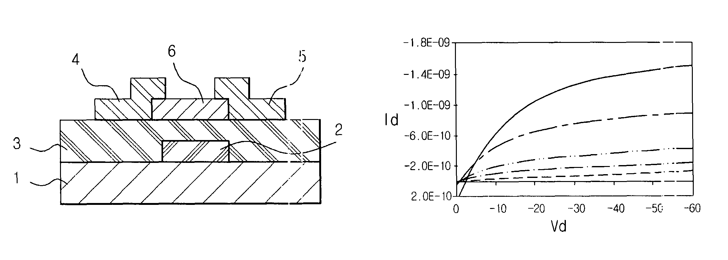
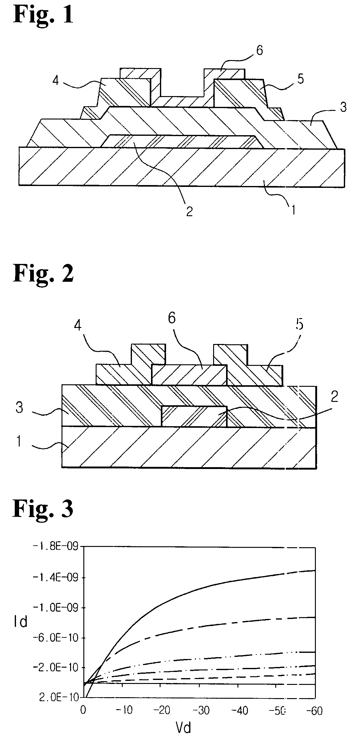
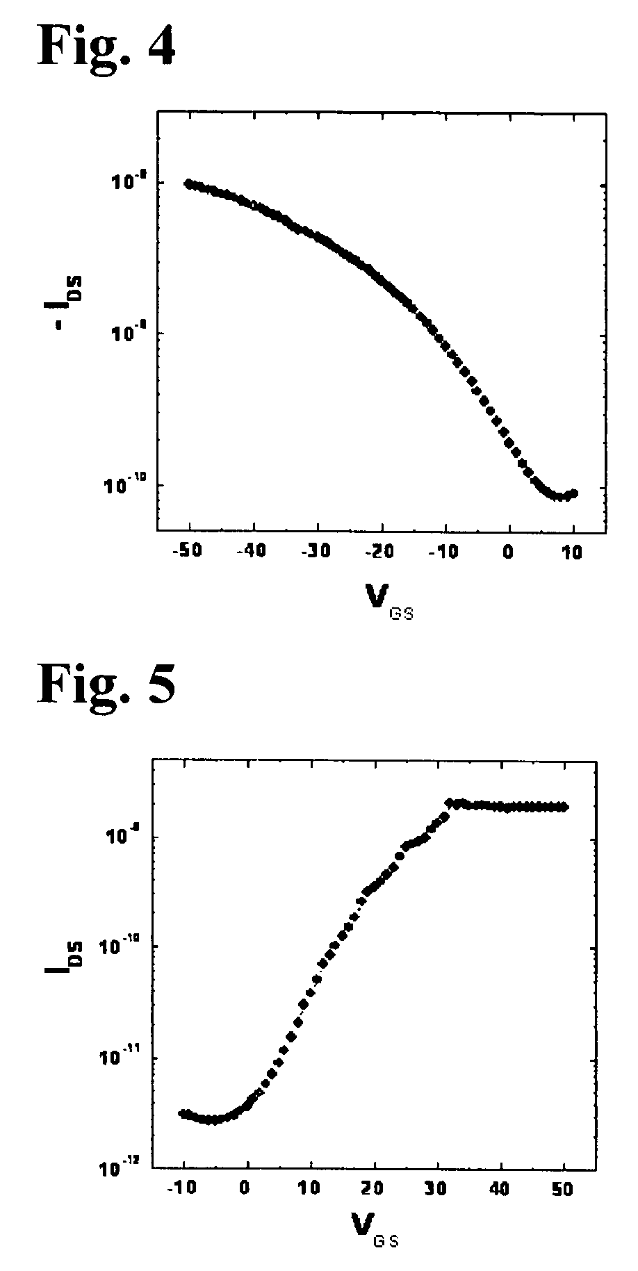

Image

  • Organic polymer semiconductor, method of preparing the same, and ambipolar organic thin film transistor using the same
  • Organic polymer semiconductor, method of preparing the same, and ambipolar organic thin film transistor using the same
  • Organic polymer semiconductor, method of preparing the same, and ambipolar organic thin film transistor using the same

Examples


example 1-a

PREPARATIVE EXAMPLE 1-a

Synthesis of 5,8-Dibromoquinoxaline Derivative (a)

[0090]To about 60 ml of a solution of 3,6-dibromo-o-phenylenediamine (about 4.0 g, about 15.0 mmol) in butanol, glacial acetic acid was added in an amount of about 2˜about 3 droplets, and then the solution was stirred at about 120° C. for about 5 hours. The resulting reaction solution was cooled to about 0° C. and filtered, and the separated solid was washed two times with hot ethanol and then dried. (Yield: about 9.6 mmol, about 64%.)

[0091]1H-NMR (300 MHz, CDCl3) δ(ppm) 3.85 (s, 6H, Phenyl-O—CH3), 6.89 (d, 4H, Phenyl-H), 7.66 (d, 4H, Phenyl-H), 7.85 (d, 2H, Quinoxaline-H).

example 1-b

PREPARATIVE EXAMPLE 1-b

Synthesis of 5,8-Dibromoquinoxaline Derivative (b)

[0092]Into a recovery flask, a 5,8-dibromoquinoxaline derivative (a) (about 4.55 g, about 9.1 mmol) and about 30 equivalents of pyridine hydrochloride (Py-HCl, about 40 g) were added, stirred at about 200° C. for about 8 hours, and then cooled to about room temperature. About 80 ml of an aqueous hydrochloric acid (about 2.5%) was added thereto, and the reaction solution was stirred well and then separated with ether. The organic layer was treated with dilute aqueous hydrochloric acid, aqueous sodium hydroxide, and aqueous hydrochloric acid, in that order, and then further separated with ether. The resultant organic layer was washed with water, and then dried using a drying agent, thereby obtaining a yellow solid. (Yield: about 8.7 mmol, about 96%.)

example 1-c

PREPARATIVE EXAMPLE 1-c

Synthesis of 5,8-Dibromoquinoxalne Derivative (c)

[0093]A solution of 5,8-dibromoquinoxalne derivative (b) (about 6.0 g, about 12.7 mmol) and aqueous potassium hydroxide (KOH, about 0.5 M, about 32 mmol) in ethanol was stirred at about room temperature for about 1 hour and then added with n-bromohexane (about 5.25 g, about 32 mmol). The reaction solution was allowed to react at about 70° C. for about 24 hours, cooled to about −20° C., and then filtered. Subsequently, column purification (development solvent: chloroform, filler: silica gel SiO2) was performed, thus obtaining a yellow solid. (Yield: about 2.2 mmol, about 51%.)

[0094]1H-NMR (300 MHz, CDCl3) δ(ppm) 0.92 (6H, CH3), 1.32˜1.50 (m, 24H, —(CH2)n—), 1.80 (m, 4H, —CH2—), 3.99 (t, 4H, Phenyl-O—CH2—), 6.87 (d, 4H, Phenyl-H), 7.64 (d, 4H, Phenyl-H), 7.85 (d, 2H, Quinoxaline-H).


PUM

PropertyMeasurementUnit
temperatureaaaaaaaaaa
semiconductoraaaaaaaaaa
ferroelectricaaaaaaaaaa

Abstract

Disclosed are an organic polymer semiconductor, an ambipolar organic thin film transistor using the same, an electronic device comprising the ambipolar organic thin film transistor and methods of fabricating the same. Example embodiments relate to an organic polymer semiconductor, which may include an aromatic ring derivative having p-type semiconductor properties and a heteroaromatic ring having n-type semiconductor properties in the main chain thereof, and which thus may exhibit both p-type transistor properties and n-type transistor properties when used in the organic active layer of an electronic device, e.g., an organic thin film transistor, an ambipolar organic thin film transistor using such an organic polymer semiconductor, an electronic device comprising the ambipolar organic thin film transistor and methods of fabricating the same.

Description

PRIORITY STATEMENT[0001]This non-provisional application claims priority under U.S.C. §119 to Korean Patent Application No. 10-2006-0105649, filed on Oct. 30, 2006, in the Korean Intellectual Property Office (KIPO), the entire contents of which are herein incorporated by reference.BACKGROUND[0002]1. Field[0003]Example embodiments relate to an organic polymer semiconductor, an ambipolar organic thin film transistor (ambipolar OTFT) using the same, an electronic device comprising the ambipolar organic thin film transistor and methods of fabricating the same. Other example embodiments relate to an organic polymer semiconductor, which may include an aromatic ring derivative having p-type semiconductor properties and a heteroaromatic ring having n-type semiconductor properties in the main chain thereof, and which thus may exhibit both p-type transistor properties and n-type transistor properties when used in the organic active layer of an electronic device, e.g., an organic thin film tra...

Claims


Application Information

Patent Timeline
Patent Type & Authority Patents(United States)
IPC IPC(8): H01L51/00
CPCC08G61/122C08G61/124C08G61/125C08G61/126H05B33/14H01L51/0036C09K11/06C09K2211/1458C09K2211/1466H01L51/0545H10K85/113H10K10/466
Inventor LEE, BANG LINLEE, EUN KYUNGHAN, KOOK MIN
Owner SAMSUNG ELECTRONICS CO LTD
Learn More