Flash memory device using ECC algorithm and method of operating the same

a flash memory and error correction code technology, applied in error detection/correction, instruments, codes, etc., can solve the problems of requiring large currents, failure in at most failure in at least one memory cell per write unit, so as to reduce the failure rate reduce the time of an erase operation, and reduce the effect of the method

Active Publication Date: 2013-01-01
SAMSUNG ELECTRONICS CO LTD
View PDF9 Cites 10 Cited by
  • Summary
  • Abstract
  • Description
  • Claims
  • Application Information

AI Technical Summary

Benefits of technology

[0014]Various aspects of the invention provide flash memory devices capable of reducing the failure rate of an erase operation and of reducing an erase time and a method of operating the same devices. In some exemplary embodiments of the invention, a control logic restarts an erase operation on an erroneously unerased data memory cell or prevents the erase operation from being restarted based on the number of erroneous bits per ECC block.

Problems solved by technology

In general, the NOR flash memory devices have the disadvantage that they require large currents.
In general, a failure occurs in at most one memory cell per write unit (e.g., per page unit).
Thus, the parity code stored in the parity cell 12 cannot be used during an erase operation of the flash memory device, so that the ECC algorithm cannot be applied to the erase operation.
As a result, when the threshold voltage of any one memory cell is not properly controlled, the entire erase operation may be failed, and an erase time may be increased due to repetition of the erase operation.

Method used


Image

  • Flash memory device using ECC algorithm and method of operating the same
  • Flash memory device using ECC algorithm and method of operating the same
  • Flash memory device using ECC algorithm and method of operating the same

Examples


Embodiment Construction

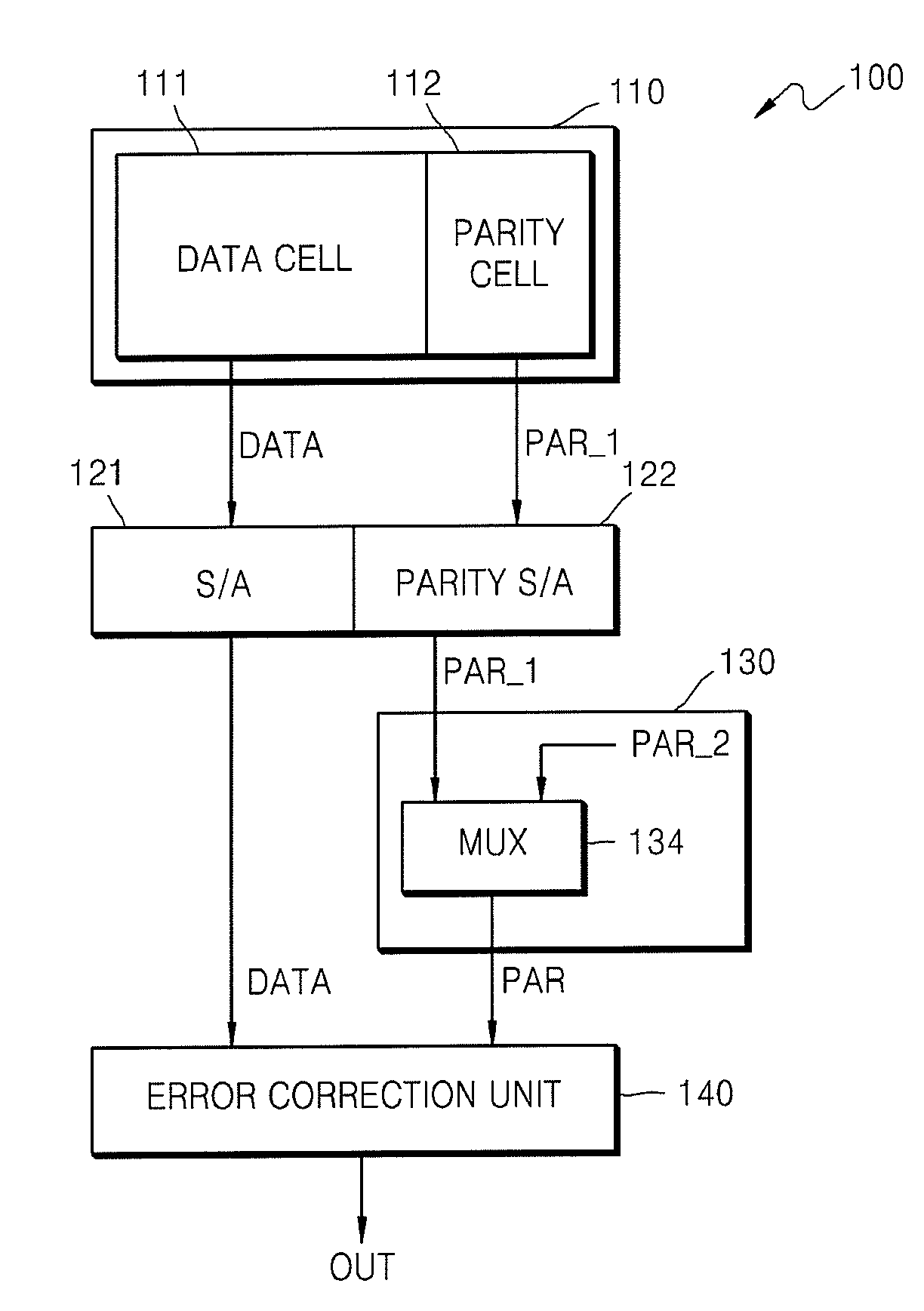
[0039]FIG. 3 is a block diagram of a flash memory device 100 according to an exemplary embodiment of the invention. Referring to FIG. 3, a flash memory device 100 may include a memory cell array 110 and peripheral circuits for performing program, read, and erase operations on the memory cells in the memory cell array 110. The memory cell array 110 may include a plurality of data memory cells 111 for storing data DATA and a corresponding parity cell 112 for storing a corresponding first parity code PAR_1 required for an error correction code (ECC) algorithm. The flash memory device 100 may include a parity generator (not shown) for generating the first parity code PAR_1. The parity generator may generate the first parity code PAR_1 corresponding to an ECC block of data (e.g., a page of data), and the generated first parity code PAR_1 may be stored in the parity cell 112. In general, the flash memory device 100 may adopt an ECC algorithm based on the Hamming code. In this case, a 1-bi...


PUM


Abstract

A flash memory device using an error correction code (ECC) algorithm and a method of operating the same. The device includes a memory cell array including a error correction code (ECC) block including data memory cells configured to store data and a parity cell configured to store a first parity code, a parity controller configured to generate a second parity code based on a the current operating mode of the flash memory device, and an error correction unit configured to receive one of the first and second parity codes and to perform an ECC algorithm on the data stored in the data memory cells using the received parity code. A control logic restarts an erase operation on an erroneously unerased data memory cell or prevents the erase operation from being restarted based on the number of erroneous bits per ECC block.

Description

CROSS-REFERENCE TO RELATED APPLICATIONS[0001]This application claims the benefit, under 35 U.S.C. §119, of Korean Patent Application No. 10-2008-0060223, filed on Jun. 25, 2008, in the Korean Intellectual Property Office, which is incorporated by reference herein in its entirety.BACKGROUND[0002]1. Field of the Invention[0003]The present invention relates to flash memory devices, and more particularly, to a flash memory device using an error correction code (ECC) algorithm.[0004]2. Description of the Related Art[0005]The demand for flash memory devices, which are nonvolatile memory devices, has increased with the popularity of mobile computer systems, cell phones, MP3 players and various other consumer electronics. A flash memory device is electrically programmable and erasable, and can retain data even if power supply is interrupted.[0006]Flash memory devices include NOR flash memory devices and NAND flash memory devices which have different methods of connecting memory cells with b...

Claims


Application Information

Patent Timeline
Patent Type & Authority Patents(United States)
IPC IPC(8): H03M13/00
CPCG06F11/1068G11C16/3454G11C16/16G11C16/02G11C29/42
Inventor YOON, CHI-WEONKIM, CHAE-HOON
Owner SAMSUNG ELECTRONICS CO LTD
Why Eureka
Try Eureka