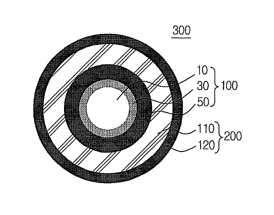
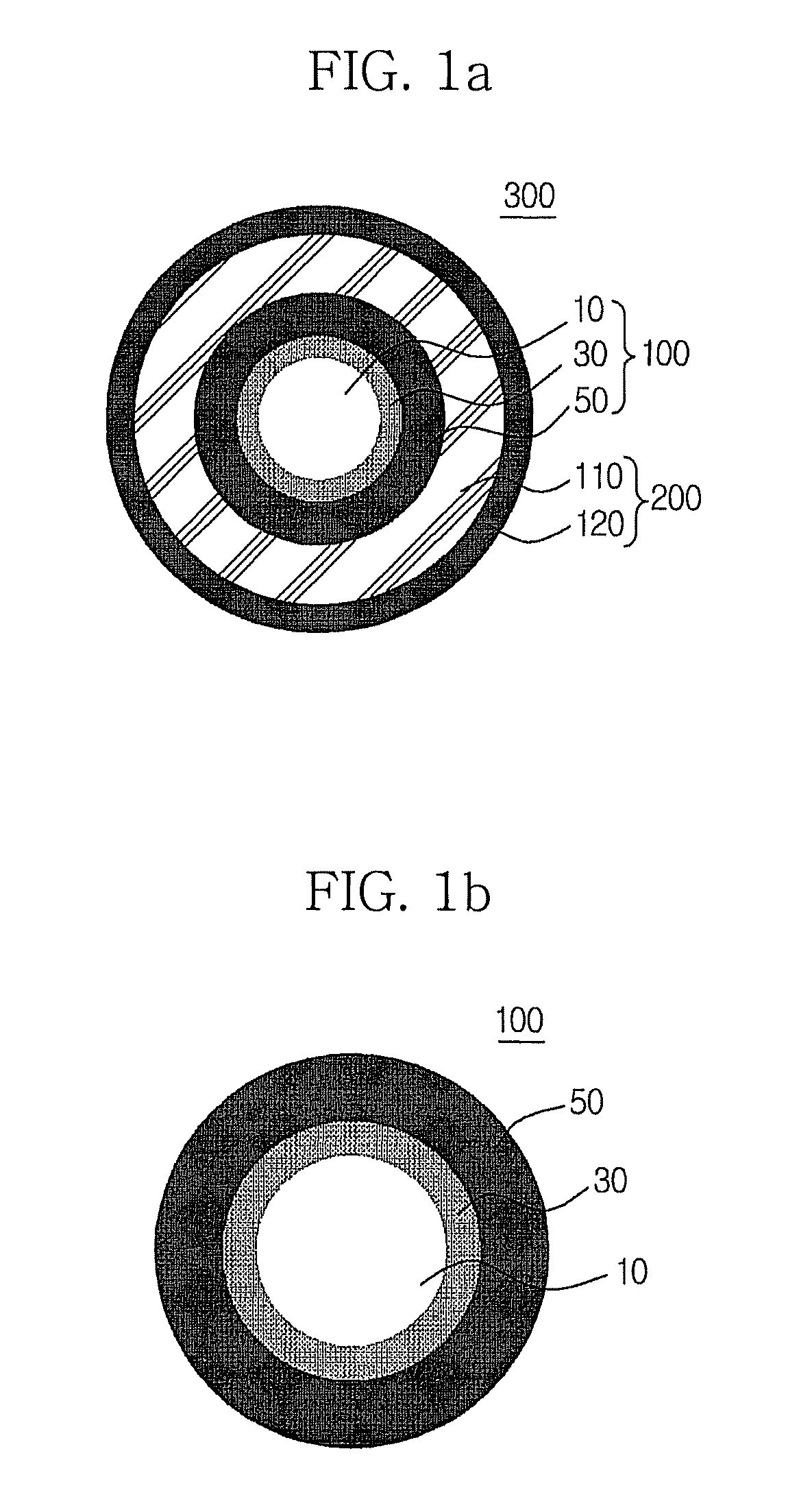
Multilayer nanocrystal structure and method for producing the same
a nanocrystal and nanocrystal technology, applied in the direction of crystal growth process, natural mineral layered products, synthetic resin layered products, etc., can solve the problems of insufficient passivation, insufficient thickness, disadvantageous aggregate of small-size nanocrystals, etc., to achieve superior chemical stability, high luminescence efficiency, and superior optical stability
- Summary
- Abstract
- Description
- Claims
- Application Information
AI Technical Summary
Benefits of technology
Problems solved by technology
Method used
Image
Examples
example 1
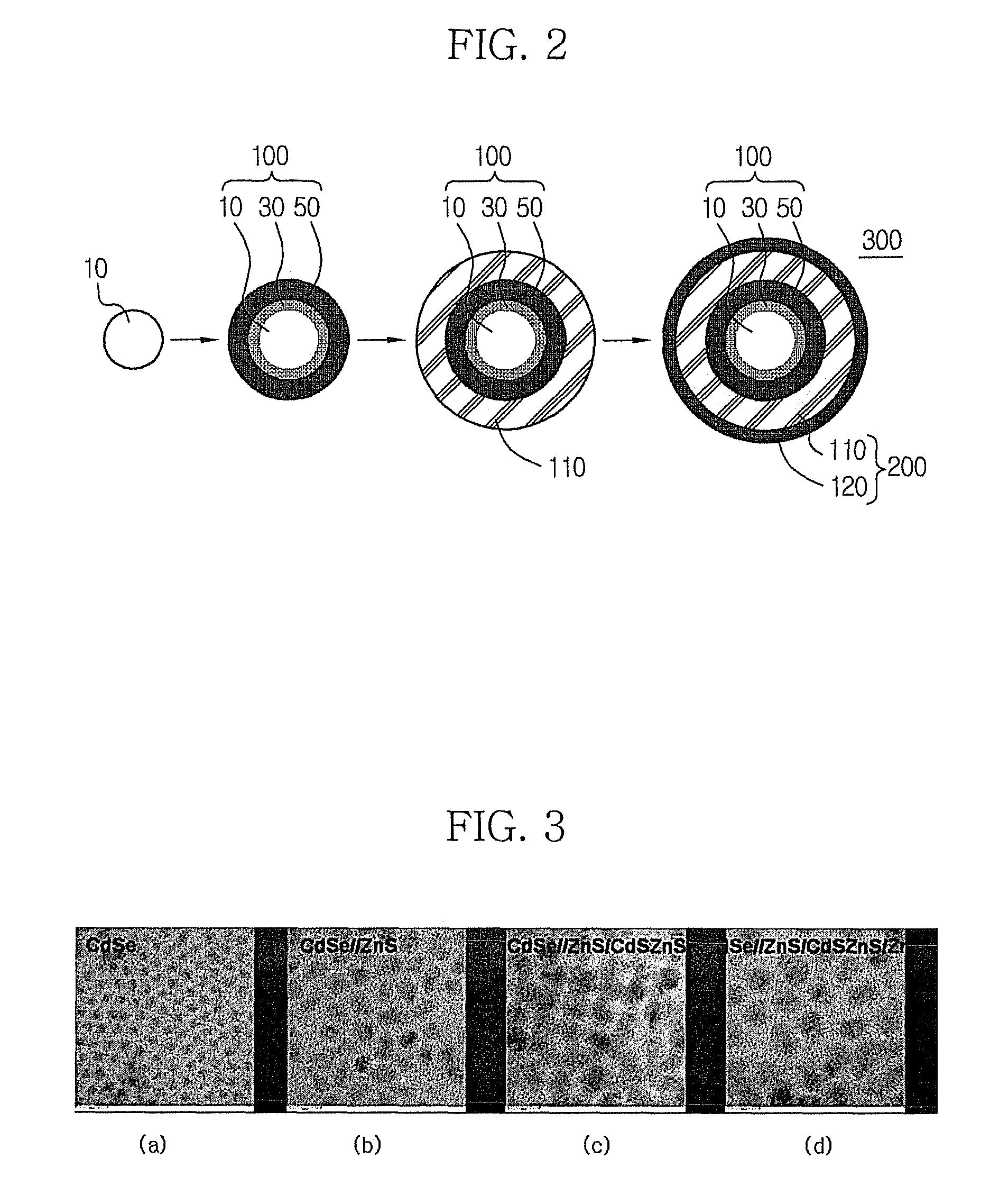
[0069]Production of CdSe / / ZnS / CdSZnS Nanocrystals
[0070]16 g of trioctylamine (hereinafter, referred to as “TOA”), 0.3 g of octadecyl phosphonic acid and 0.4 mmol of cadmium oxide were simultaneously placed in a 125 ml flask equipped with a reflux condenser. The reaction temperature of the mixture was adjusted to 300° C. with stirring.
[0071]Separately, selenium (Se) powder was dissolved in trioctylphosphine (“TOP”) to obtain a Se-TOP complex solution (Se concentration: about 2 M), and 2 ml of the Se-TOP complex solution was rapidly fed to the previous reaction mixture. The reaction was continued for about 2 minutes.
[0072]After completion of the reaction, the reaction mixture was cooled to room temperature as rapidly as possible. Ethanol (10 ml) as a non-solvent was added to the reaction mixture, and then the resulting mixture was centrifuged. The obtained precipitate was separated from the supernatant, and dispersed in toluene (4 ml) to prepare a solution of a CdSe nanocrystal having...
example 2
[0080]Production of CdSe / / ZnS / CdSZnS Nanocrystals with Controlled Band Gap
[0081]8 g of TOA, 0.1 g of oleic acid, 0.1 mmol of cadmium oxide and 0.4 mmol of zinc acetate were simultaneously placed in a 125 ml flask equipped with a reflux condenser. The reaction temperature of the mixture was adjusted to 300° C. with stirring. After 2 ml of the CdSe / / ZnS nanocrystal solution prepared in Example 1 was added to the reaction mixture, 1 ml of an S-TOP complex solution (0.8 M of sulfur in TOP) was slowly added thereto. The reaction was continued for about one hour to grow a CdSZnS nanocrystal on the CdSe / / ZnS nanocrystal to produce a CdSe / / ZnS / CdSZnS nanocrystal that emits light at a wavelength of 554 nm.
[0082]After the reaction was completed, the reaction mixture was cooled to room temperature as rapidly as possible. Ethanol (10 ml) as a non-solvent was added to the reaction mixture, and the resulting mixture was centrifuged. The obtained precipitate was separated from the supernatant, and...
example 3
[0083]Production of CdSe / / ZnS / CdSZnS Nanocrystals According to Changes in Band Gap
[0084]8 g of TOA, 0.1 g of oleic acid, 0.2 mmol of cadmium oxide and 0.4 mmol of zinc acetate were simultaneously placed in a 125 ml flask equipped with a reflux condenser. The reaction temperature of the mixture was adjusted to 300° C. with stirring. After the CdSe / / ZnS nanocrystal solution prepared in Example 1 was added to the reaction mixture, 1 ml of an S-TOP complex solution (0.8 M of sulfur in TOP) was slowly added thereto. The reaction was continued for about one hour to grow a CdSZnS nanocrystal on the CdSe / / ZnS nanocrystal to produce a CdSe / / ZnS / CdSZnS nanocrystal that emits light at a wavelength of 570 nm.
[0085]After the reaction was completed, the reaction mixture was cooled to room temperature as rapidly as possible. Ethanol (10 ml) as a non-solvent was added to the reaction mixture, and the resulting mixture was centrifuged. The obtained precipitate was separated from the supernatant, and...
PUM
| Property | Measurement | Unit |
|---|---|---|
| temperature | aaaaa | aaaaa |
| thickness | aaaaa | aaaaa |
| thickness | aaaaa | aaaaa |
Abstract
Description
Claims
Application Information
 - R&D
- Intellectual Property
- Life Sciences
- Materials
- Tech Scout
- Unparalleled Data Quality
- Higher Quality Content
- 60% Fewer Hallucinations
Browse by: Latest US Patents, China's latest patents, Technical Efficacy Thesaurus, Application Domain, Technology Topic, Popular Technical Reports.
© 2025 PatSnap. All rights reserved.Legal|Privacy policy|Modern Slavery Act Transparency Statement|Sitemap|About US| Contact US: help@patsnap.com


