
Integrated circuit having a bulk acoustic wave device and a transistor

a technology of integrated circuits and transistors, which is applied in the direction of semiconductor devices, semiconductor/solid-state device details, electrical equipment, etc., can solve the problems of filtering occupying a lot of space and being difficult to integrate with transistors

Active Publication Date: 2012-11-06
NXP USA INC
View PDF5 Cites 96 Cited by
  • Summary
  • Abstract
  • Description
  • Claims
  • Application Information

AI Technical Summary

Problems solved by technology

However, SAW filters take up a lot of space and are difficult to integrate with transistors.

Method used


Image

  • Integrated circuit having a bulk acoustic wave device and a transistor
  • Integrated circuit having a bulk acoustic wave device and a transistor
  • Integrated circuit having a bulk acoustic wave device and a transistor

Examples


Embodiment Construction

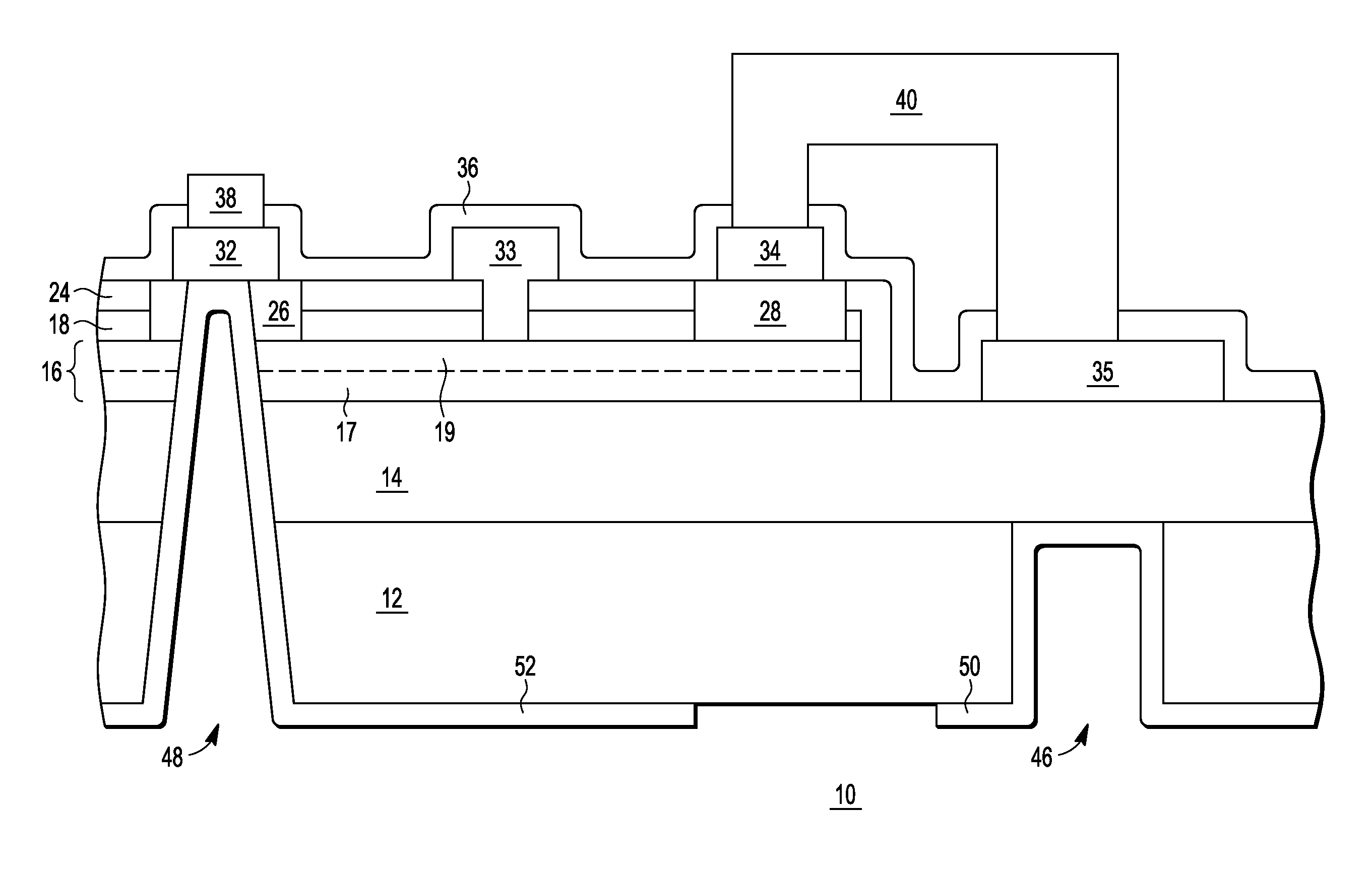
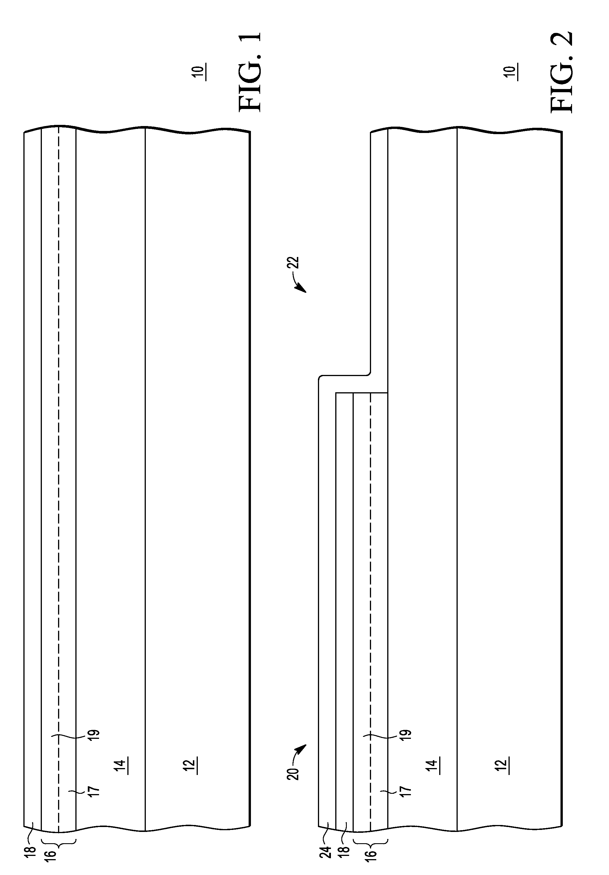
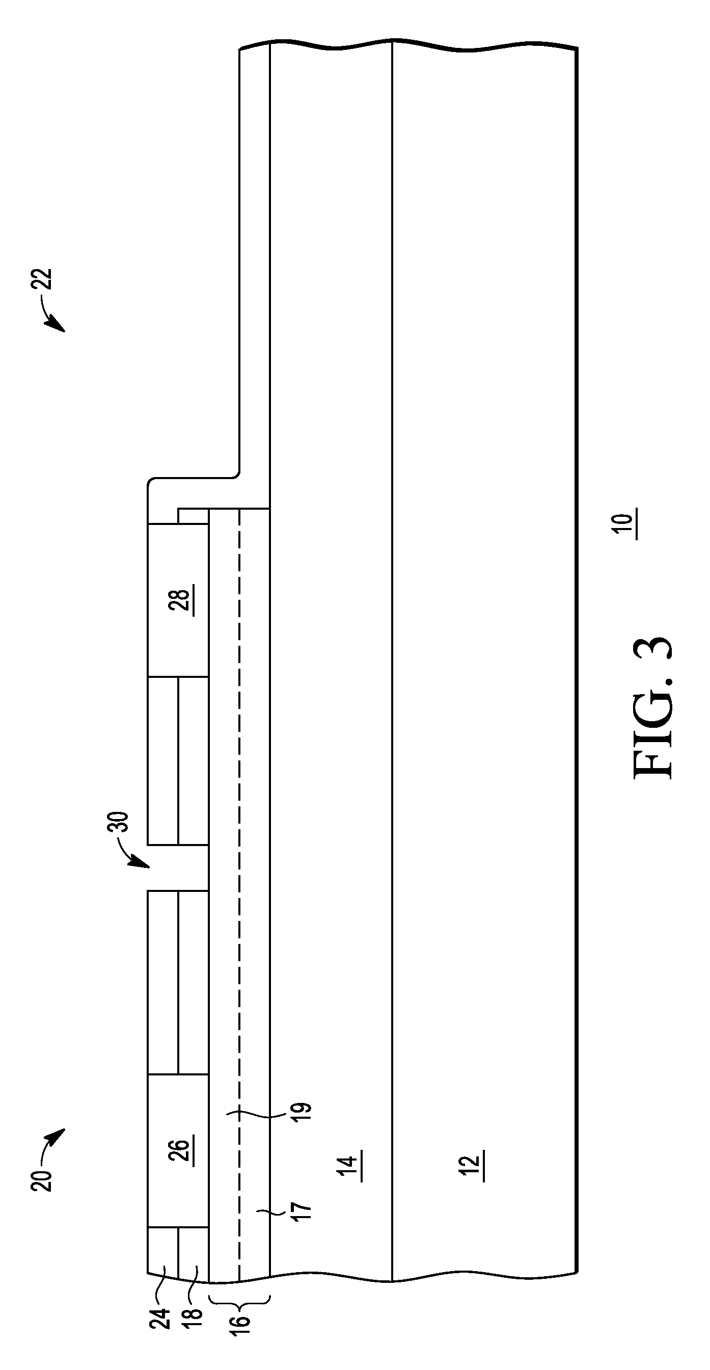
[0015]By integrating a bulk acoustic waver (BAW) device, which is more compact than an SAW filter and has improved performance at frequencies greater than 2 GHz unlike the SAW filters, with a GaN transistor, an improved RF integrated circuit can be achieved. The use of an epitaxial GaN layer improves the performance of a BAW resonator. GaN is an expensive material and RF devices are still typically manufactured on small wafers (approximately 3 inch wafers) so the use of a smaller device saves cost and allows for manufacturing to still continue using small wafers. Furthermore, through vias are used in the integration. Hence, bulk micro-machined GaN BAW filters are integrated with GaN transistors to reduce the total device area provided by integrating these two functions on one integrated circuit chip.

[0016]FIG. 1 illustrates a portion of an integrated circuit 10 in accordance with an embodiment. The integrated circuit 10 includes a semiconductor substrate 12, a GaN layer 14, a barrie...


PUM


Abstract

A bulk GaN layer is on a first surface of a substrate, wherein the bulk GaN layer has a GaN transistor region and a bulk acoustic wave (BAW) device region. A source / drain layer is over a first surface of the bulk GaN layer in the GaN transistor region. A gate electrode is formed over the source / drain layer. A first BAW electrode is formed over the first surface of the bulk GaN layer in the BAW device region. An opening is formed in a second surface of the substrate, opposite the first surface of the substrate, which extends through the substrate and exposes a second surface of the bulk GaN layer, opposite the first surface of the bulk GaN layer. A second BAW electrode is formed within the opening over the second surface of the bulk GaN layer.

Description

BACKGROUND[0001]1. Field[0002]This disclosure relates generally to forming a bulk acoustic wave device and a transistor.[0003]2. Related Art[0004]In RF (radio frequency) applications, power amplification and filtering functions are important. Typically, filtering is achieved using an integrated circuit having a surface acoustic wave (SAW) filter and another integrated circuit having a transistor. However, as the industry desires to decrease the real estate of integrated circuits, there is a desire to have SAW filters and transistors formed on the same integrated circuit. However, SAW filters take up a lot of space and are difficult to integrate with transistors.BRIEF DESCRIPTION OF THE DRAWINGS[0005]The present invention is illustrated by way of example and is not limited by the accompanying figures, in which like references indicate similar elements. Elements in the figures are illustrated for simplicity and clarity and have not necessarily been drawn to scale.[0006]FIG. 1 illustra...

Claims


Application Information

Patent Timeline
Patent Type & Authority Patents(United States)
IPC IPC(8): H01L21/00
CPCH01L29/2003H01L29/41725H01L29/66856H01L29/7786H01L29/812H03H9/0542
Inventor HUANG, JENN HWAGREEN, BRUCE M.
Owner NXP USA INC
Learn More