Pressure sensor and manufacturing method

a manufacturing method and sensor technology, applied in the direction of fluid pressure measurement, fluid pressure measurement by electric/magnetic elements, instruments, etc., can solve the problems of difficult control of the height to which solder is applied, affecting the semiconductor substrate, and difficult control of the range over which the metal thin film is placed, so as to suppress more effectively the occurrence of characteristic defects, and increase the strength of bonding

Active Publication Date: 2012-07-17
YAMATAKE HONEYWELL CO LTD
View PDF8 Cites 11 Cited by
  • Summary
  • Abstract
  • Description
  • Claims
  • Application Information

AI Technical Summary

Benefits of technology

[0010]In the first aspect according to the present invention, the second diameter for the pressure introducing hole at the top surface of the glass pedestal is larger than the first diameter for the pressure introducing hole at the bottom surface of the glass pedestal. Because of this, it is possible to prevent the deposition of the metal thin film layer on the side walls of the pressure introducing hole on the semiconductor substrate side, even when depositing the metal thin film layer on the bottom surface of the glass pedestal. Doing so makes it possible to prevent the creeping of the solder on the side walls of the pressure introducing hole on the semiconductor substrate side. This makes it possible to suppress more effectively the characteristic defects that occur due to the creeping of the solder near to the semiconductor substrate.
[0029]The present invention is not only able to suppress more effectively the occurrence of characteristic defects, but also able to increase the strength of bonding between the glass pedestal and the metal base.

Problems solved by technology

Moreover, it is difficult to control the range over which the metal thin film layer is deposited onto the side wall of the pressure introducing hole.
Because of this, it is difficult to control the height to which the solder creeps up the side wall portion of the pressure introducing hole.
Doing so can affect the semiconductor substrate, such as causing stresses (thermal stresses) caused by differences in coefficients of thermal expansion between the solder and the semiconductor substrate.
Additionally, these thermal stresses, and the like, may lead to defects in the characteristics of the semiconductor substrate.
Because of this, it is possible that the strength of bonding between the glass pedestal and the metal base will be inadequate.
Furthermore, in the pressure sensor as set forth in JP '972, the excess solder will pool in the pressure introducing hole, so the pressure introducing hole may become blocked with solder.

Method used


Image

  • Pressure sensor and manufacturing method
  • Pressure sensor and manufacturing method
  • Pressure sensor and manufacturing method

Examples


Embodiment Construction

[0041]A form of embodiment according to the present invention will be explained below in reference to the drawings.

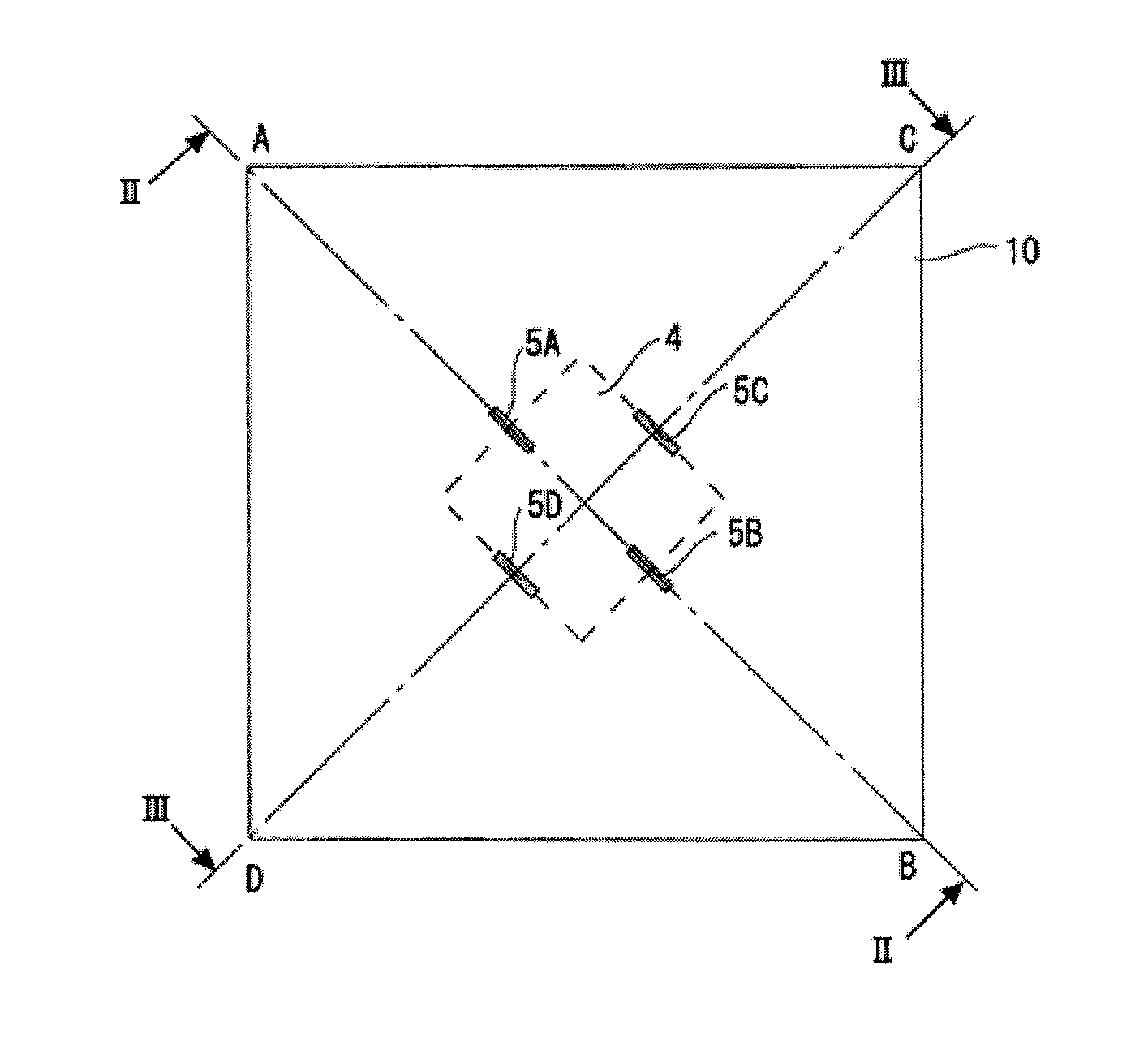
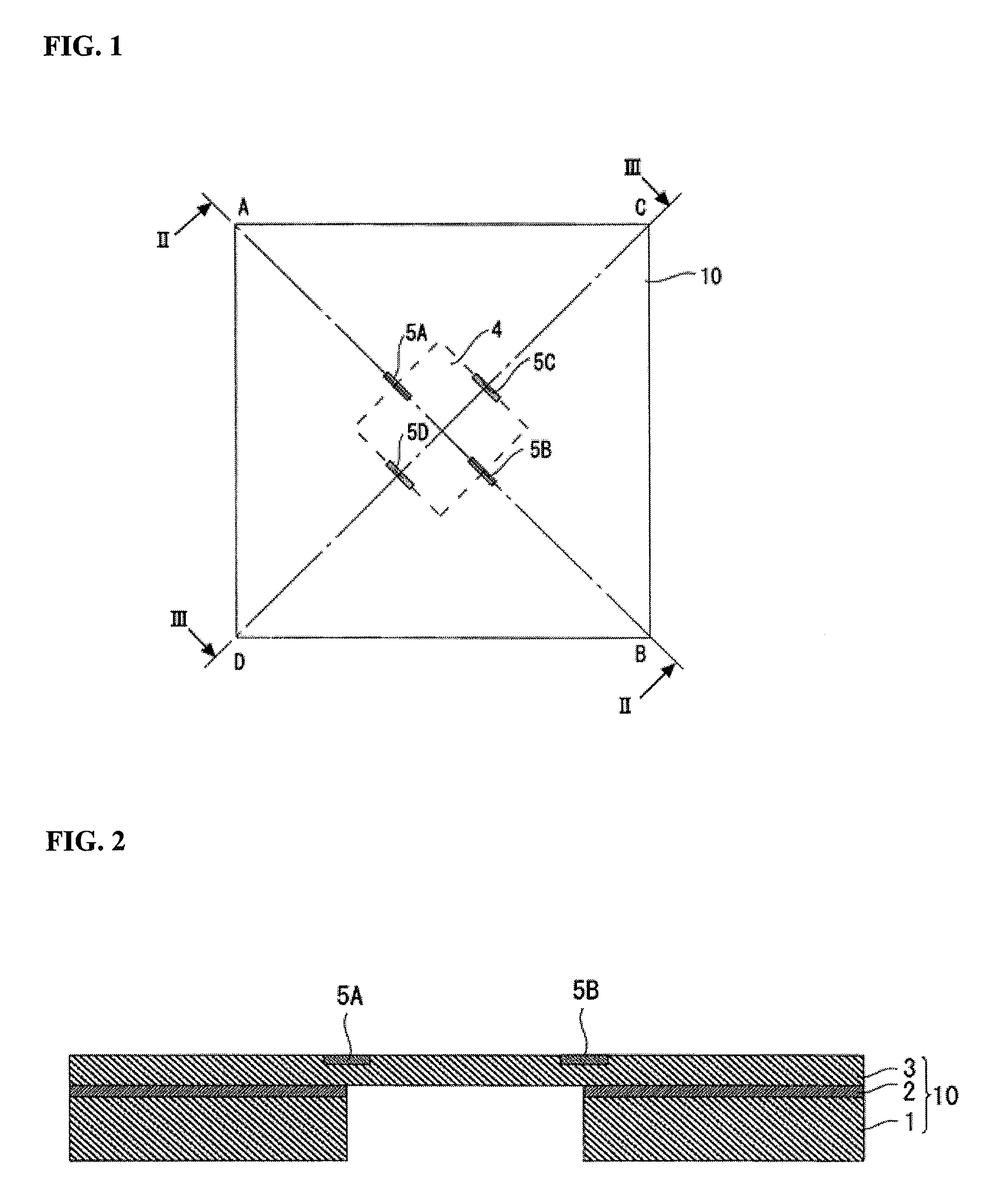
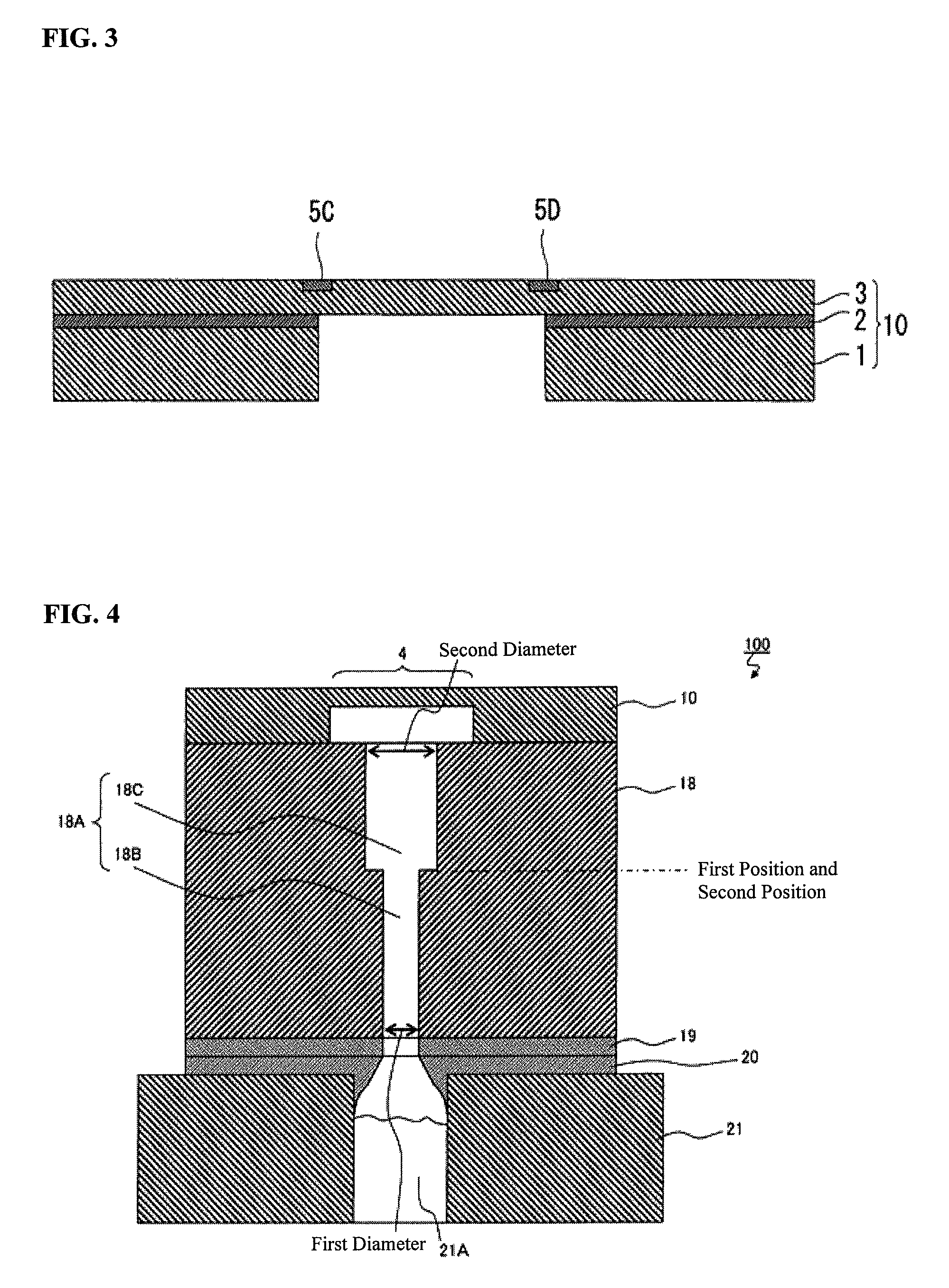
[0042]In the below, a specific form of embodiment wherein the present invention is applied will be explained in detail while referencing the drawings. FIG. 1 is a top view illustrating the structure of a sensor chip 10 (a semiconductor substrate) used in a pressure sensor 100 according to the present form of embodiment. FIG. 2 is a cross-sectional diagram along the section II-II in FIG. 1, and FIG. 3 is a cross-sectional diagram along the section III-III. The pressure sensor 100 according to the present form of embodiment is a semiconductor sensor that uses the piezoresistance effect of semiconductors.

[0043]The pressure sensor 100 has a sensor chip 10 that is made out of a semiconductor substrate. The sensor chip 10 is a square shape. As illustrated in FIG. 1, the corners of the square sensor chip 10 are defined as A, B, C, and D. As illustrated in FIG. 1, the upper-lef...


PUM

PropertyMeasurementUnit
thicknessaaaaaaaaaa
pressureaaaaaaaaaa
diameteraaaaaaaaaa

Abstract

A semiconductor substrate, provided with a differential pressure diaphragm, and a glass pedestal, which is provided on the bottom side of the semiconductor substrate, are provided, wherein: the bottom surface of the semiconductor substrate and the top surface of the glass pedestal are bonded together; a pressure introducing hole is formed in the glass pedestal so as to pass through the glass pedestal, connecting between the top and bottom surfaces of the glass pedestal; the pressure introducing hole is formed with a first diameter for the pressure introducing hole at the bottom surface of the glass pedestal from the bottom surface of the glass pedestal to a first position; and a second diameter for the pressure introducing hole at the top surface of the glass pedestal is larger than the first diameter; where a metal thin film layer is deposited on the bottom surface of the glass pedestal.

Description

CROSS REFERENCE TO RELATED APPLICATIONS[0001]The present application claims priority under 35 U.S.C. §119 to Japanese Patent Application No. 2009-159761, filed Jul. 6, 2009, which is incorporated herein by reference.FIELD OF TECHNOLOGY[0002]The present invention relates to a pressure sensor and to a manufacturing method, and, in particular, relates to a pressure sensor having a diaphragm, and to a method for manufacturing that pressure sensor.BACKGROUND OF THE INVENTION[0003]Pressure sensors that use a semiconductor piezoresistance effect are small and light, and have high sensitivity, and thus are used broadly in fields such as industrial instrumentation and medicine. This type of pressure sensor includes a semiconductor substrate that is provided with a diaphragm portion, a glass pedestal wherein is formed a pressure introducing hole, and a metal base (a stem). Additionally, the semiconductor substrate is bonded to the top surface of the glass pedestal using an anode bonding metho...

Claims


Application Information

Patent Timeline
Patent Type & Authority Patents(United States)
IPC IPC(8): G01L9/00
CPCG01L9/0042G01L19/147
Inventor TOJO, HIROFUMI
Owner YAMATAKE HONEYWELL CO LTD
Why Eureka
Try Eureka