
Package manufacturing method, package, optical module and die for integral molding

a technology of optical modules and manufacturing methods, applied in manufacturing tools, semiconductor lasers, instruments, etc., can solve the problems of difficult manufacturing at the required positional accuracy, easy production of warps at the mounting surface of optical elements,

Inactive Publication Date: 2012-07-10
ORMON CORP
View PDF8 Cites 8 Cited by
  • Summary
  • Abstract
  • Description
  • Claims
  • Application Information

AI Technical Summary

Benefits of technology

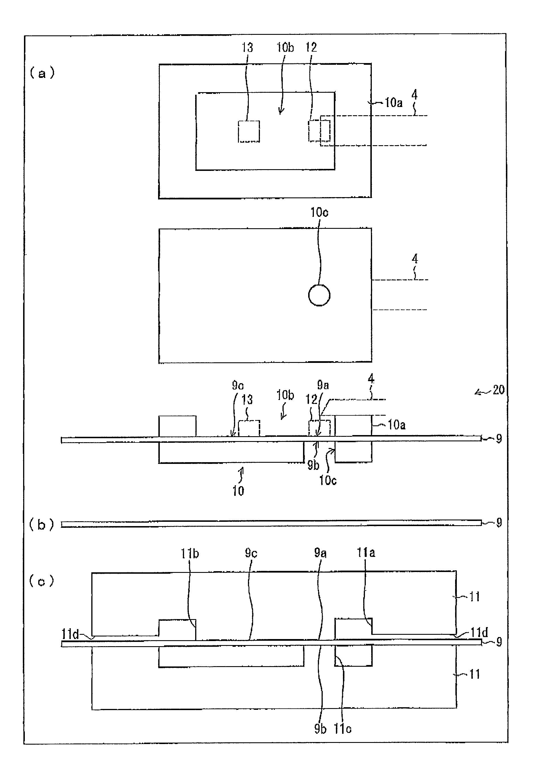
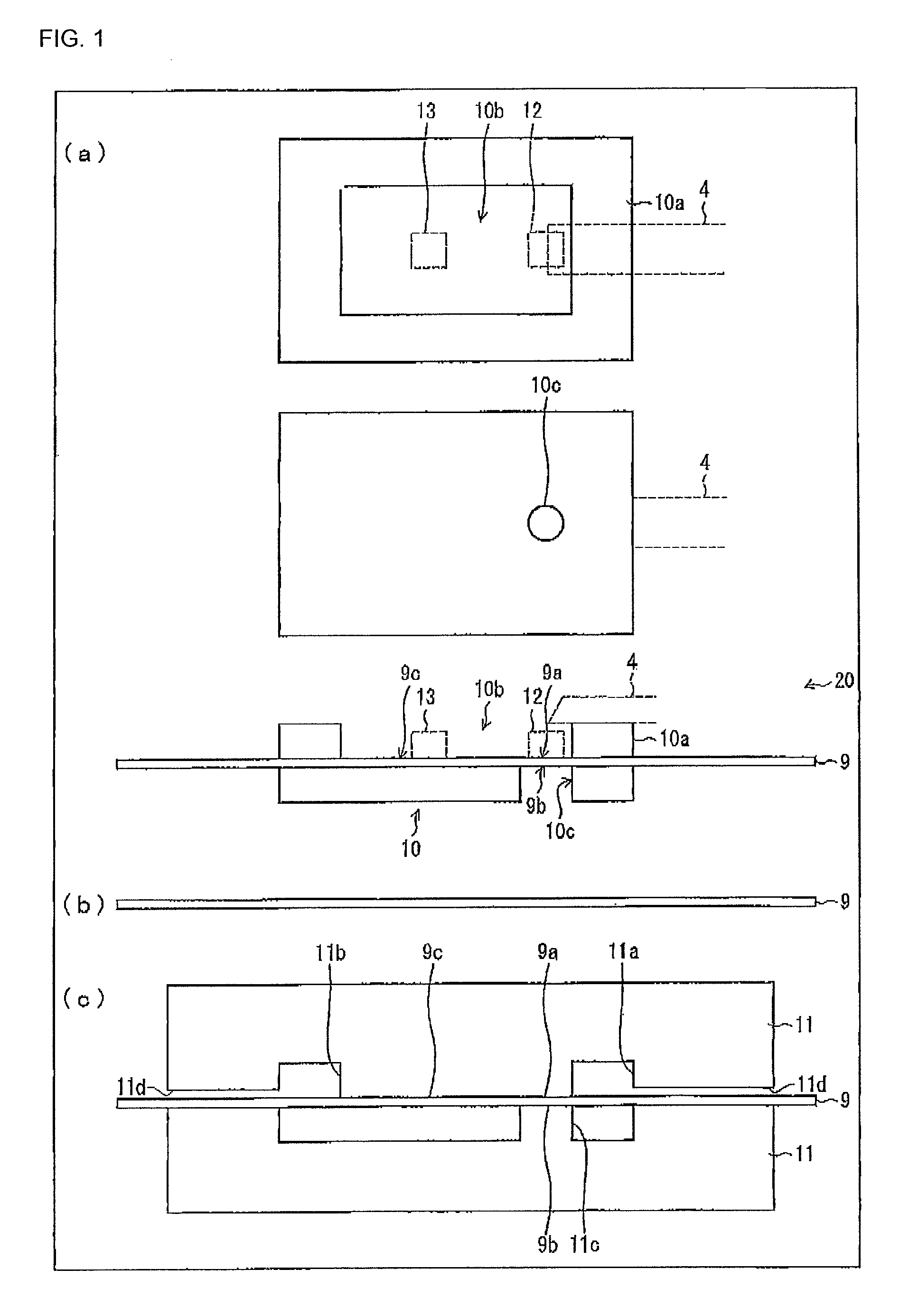
The present invention provides a manufacturing method of a package, a package, an optical module, and an integrally molding die that can meet the positional accuracy requirements for maintaining the positional relationship of the flexible light transmission path end and the optical element constant. This is achieved by using an integrally molding die with a recess for forming the supporting portion, a first projection, and a second projection that come into contact with both the optical element mounting surface and the back surface of the optical element mounting surface, ensuring a flat surface for the optical element mounting portion of the lead frame during the molding process. The package and optical module manufactured through this method can prevent warp of the optical element mounting surface and satisfy the positional accuracy requirements.

Problems solved by technology

However, the techniques disclosed in Patent Documents 1 and 2 have the following problems when applied to the manufacturing method of the package mounted with the light transmission path and the optical element.
Thus, the warp tends to easily produce at the optical element mounting surface, and manufacturing at the demanded positional accuracy becomes difficult even if the technique disclosed in Patent Document 1 is applied and the package is manufactured with the four portions of the optical element mounting surface in the lead frame held down with the upper and lower movable pins.

Method used


Image

  • Package manufacturing method, package, optical module and die for integral molding
  • Package manufacturing method, package, optical module and die for integral molding
  • Package manufacturing method, package, optical module and die for integral molding

Examples


application example

(Application Example)

[0073]The optical module 1 of the present embodiment can be applied to the following application examples.

[0074]First, as a first application example, use can be made at a hinge portion in a foldable electronic device such as a foldable portable telephone, a foldable PHS (Personal Handyphone System), a foldable PDA (Personal Digital Assistant), and a foldable notebook computer.

[0075]FIGS. 8 (a) to (c) show an example in which the light guide 4 is applied to a foldable portable telephone 40. In other words, FIG. 8(a) is a perspective view showing an outer appearance of the foldable portable telephone 40 incorporating the light guide 4.

[0076]FIG. 8(b) is a block diagram of a portion where the light guide 4 is applied in the foldable portable telephone 40 shown in FIG. 8(a). As shown in the figure, a control unit 41 arranged on a body 40a side in the foldable portable telephone 40, an external memory 42, a camera (digital camera) 43, and a display unit (liquid crys...


PUM

PropertyMeasurementUnit
inclined angleaaaaaaaaaa
shapeaaaaaaaaaa
speedaaaaaaaaaa

Abstract

An integrally molding die for manufacturing a package includes a supporting portion for supporting at least one end including an incident / exit port of a light signal in a light transmission path, and a lead frame for mounting an optical element. The integrally molding die includes a recess for forming the supporting portion, a first projection, which comes into contact with an optical element mounting surface of the lead frame, and a second projection, which comes into contact with a back surface of the optical element mounting surface.

Description

TECHNICAL FIELD[0001]The present invention relates to a method of manufacturing a package, a package, an optical module, and an integrally molding die.BACKGROUND ART[0002]In recent years, optical communication network enabling large capacity data communication at high speed is expanding. The optical communication network is assumed to be mounted on a consumer device in the future. An electrical input / output optical data transmission cable (optical cable) capable of being used no different from the present electrical cable is desired for the application of large capacity data transfer at higher speed, noise countermeasures, and data transmission between substrates in the device. In view of flexibility, a light guide is desirably used for the optical cable. A light transmission path will be described below as the light guide, but includes light transmission paths such as an optical fiber.[0003]The light guide is formed by a core having a large index of refraction and a clad having a s...

Claims


Application Information

Patent Timeline
Patent Type & Authority Patents(United States)
IPC IPC(8): G02B6/12G02B6/255B28B23/18
CPCG02B6/122G02B6/4203H01L21/565H01L31/0203H01S5/02248H04M1/026H01L2924/0002H01L2924/00H01S5/02325
Inventor SANO, AKIHIKONOZAWA, HIROTOYASUDA, NARUHOSOKAWA, HAYAMI
Owner ORMON CORP
Learn More