Non-volatile memory low voltage and high speed erasure method
a non-volatile memory, high-speed erasure technology, applied in the direction of digital storage, instruments, semiconductor devices, etc., can solve the problems of manufacturing difficulties, increase of costs, and inability to achieve the purpose of low voltage and high-speed erasure, etc., to achieve high reliability, low operation current, and low operation voltage.
- Summary
- Abstract
- Description
- Claims
- Application Information
AI Technical Summary
Benefits of technology
Problems solved by technology
Method used
Image
Examples
first embodiment
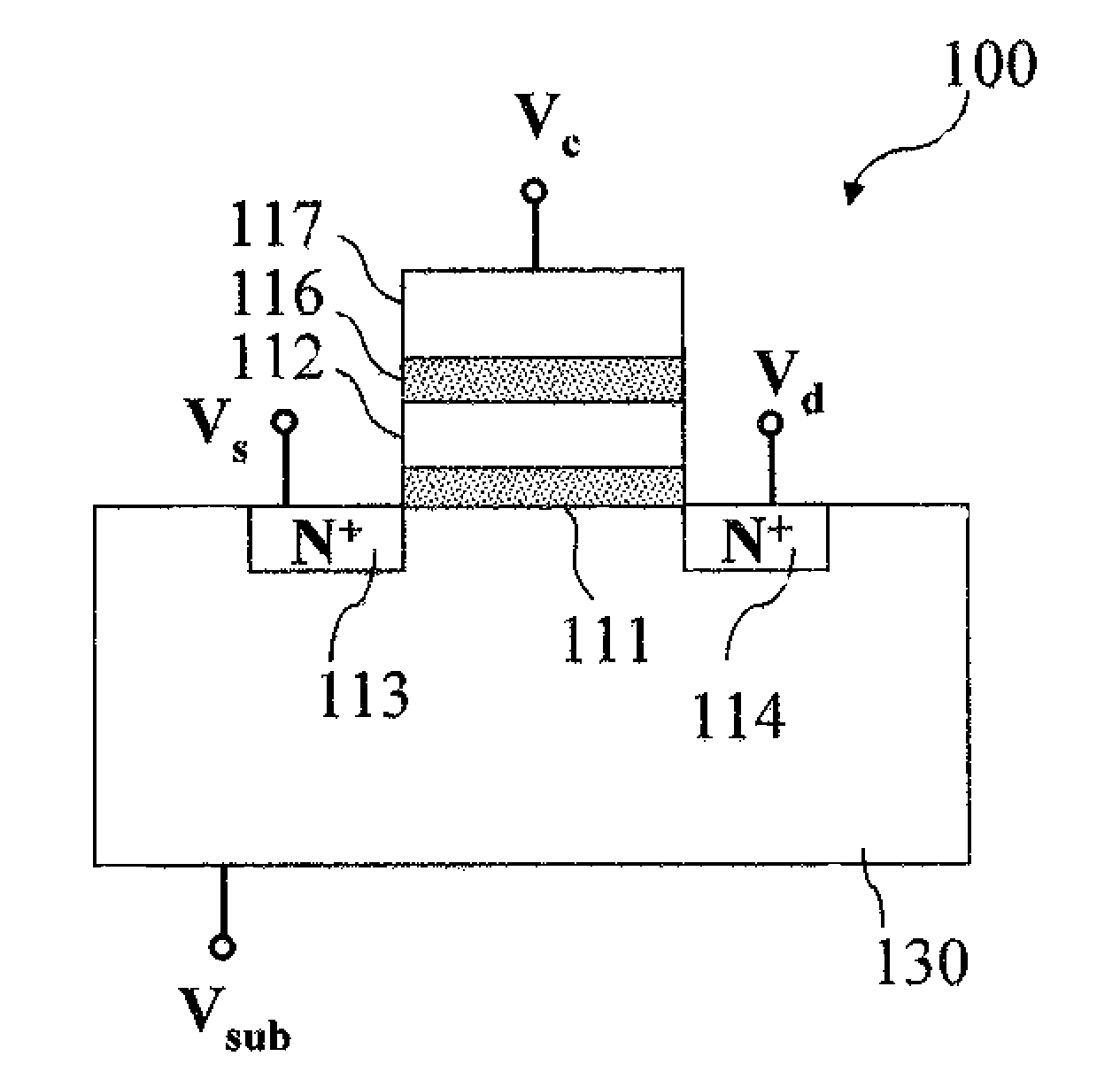
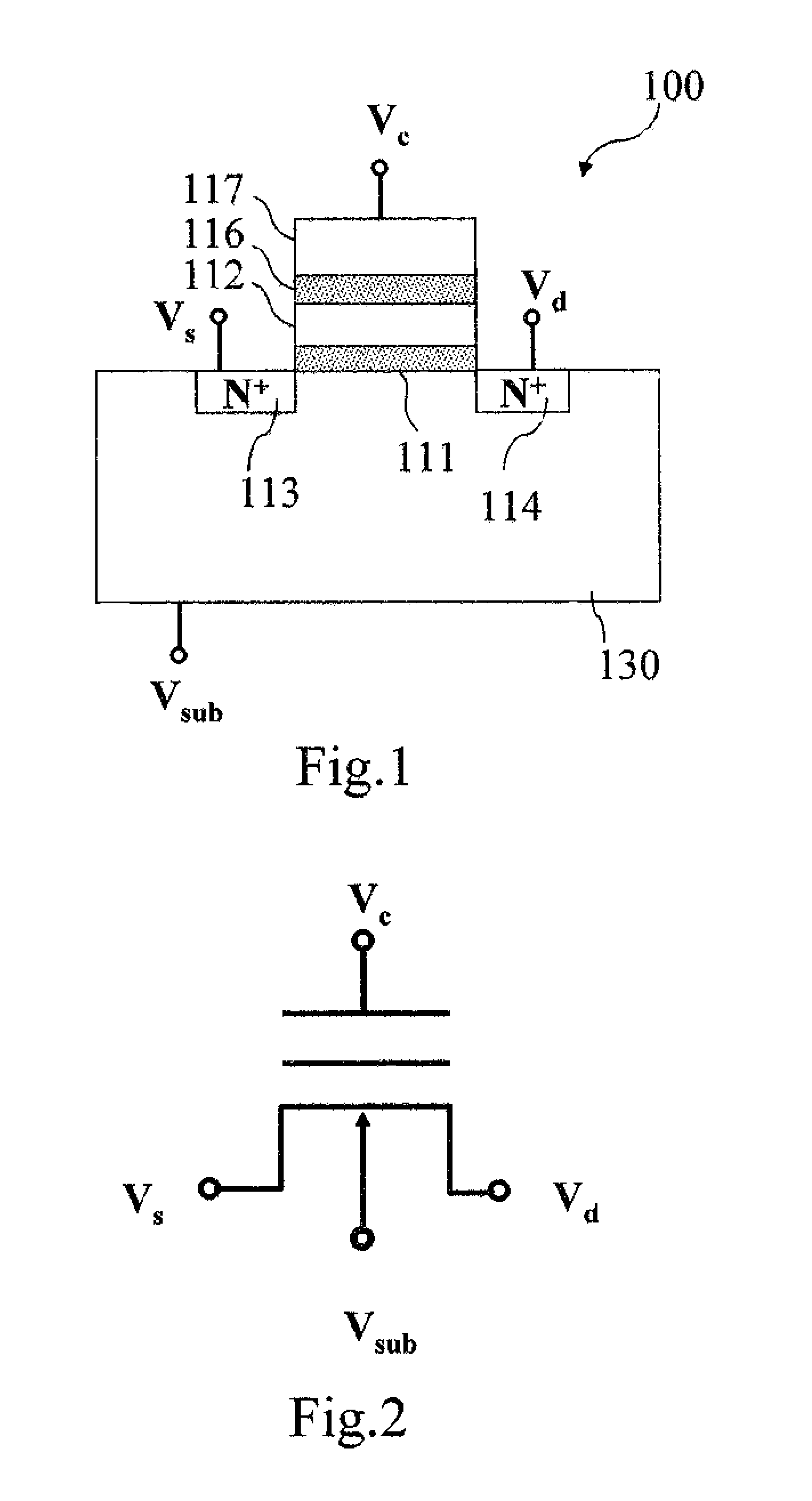
[0019]Refer to FIG. 1 for a cross section view of a non-volatile memory structure according to the present invention. As shown in FIG. 1, the non-volatile memory structure 100 includes: a stacked gate structure disposed in a P-type semiconductor substrate 130. The stacked gate structure includes: a floating gate 112 stacked on a tunneling dielectric layer 111, a control gate 117 disposed above the floating gate 112 through a gate dielectric layer 116, and a source 113 and a drain 114 disposed in a P-type semiconductor substrate 130. Wherein, the source 113 and the drain 114 are N-type ion-doped regions.
[0020]As shown in FIG. 1, the non-volatile memory structure 100 is a structure having four terminals: a source, a drain, a controlling gate, and a substrate connection structure respectively, such that a substrate voltage Vsub, a source voltage Vs, a drain voltage Vd, and a control gate voltage Vc are applied on the substrate 130, the source 113, the drain 114, and the control gate 11...
second embodiment
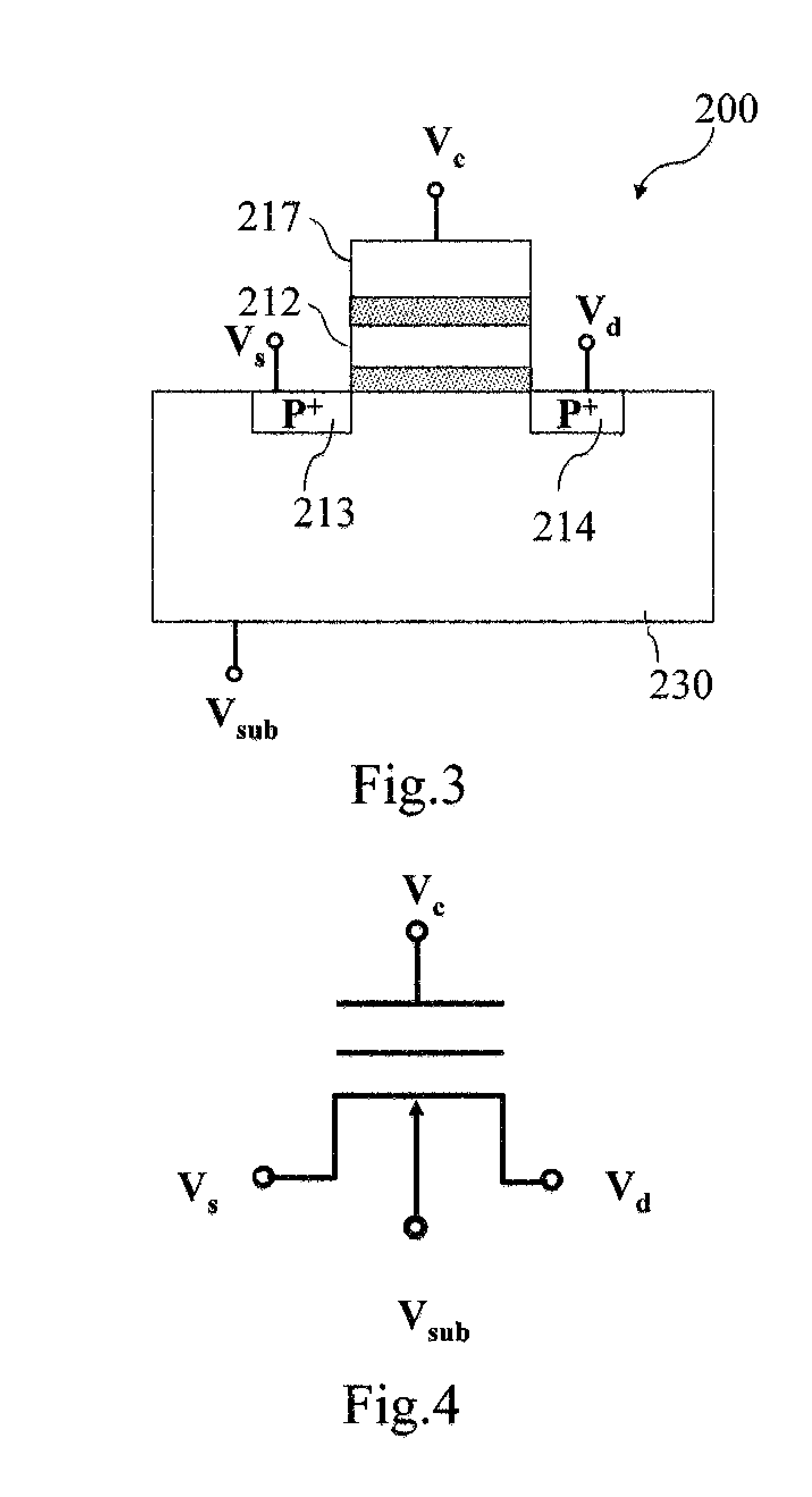
[0028]FIG. 3 is a cross section view of a non-volatile memory structure according to the present invention. As shown in FIG. 3, the non-volatile memory structure 200 of the present invention can be realized through forming a stacked gate structure in an N-type semiconductor substrate 230, such that the source 213 and the drain 214 are P-type ion-doped regions, and the stacked gate structure includes a control gate 217 stacked above a floating gate 212.
[0029]In performing low voltage and high speed erasure process to the non-volatile memory structure 200, the erasure is achieved through applying substrate voltage Vsub, source voltage Vs, drain voltage Vd, and control gate voltage Vc on the substrate 230, the source 213, drain 214, and the control gate 217 respectively. FIG. 4 is an equivalent circuit diagram of a non-volatile memory structure of FIG. 3 according to a second embodiment of the present invention, such that the operation conditions of the low voltage and high speed erasu...
third embodiment
[0034]FIG. 5 is a cross section view of a non-volatile memory structure according to the present invention. As shown in FIG. 5, the non-volatile memory structure 300 of the present invention can be realized through forming a stacked gate structure in an N-type semiconductor substrate 330, such that the source 313 and the drain 314 are P-type ion-doped regions, a P-type well is provided underneath the source 313 and the drain 314, and the stacked gate structure includes a control gate 317 stacked above a floating gate 312.
[0035]In performing low voltage and high speed erasure process to the non-volatile memory structure 300, the erasure is achieved through applying substrate voltage Vsub, P-type well voltage Vpwell, source voltage Vs, drain voltage Vd, and control gate voltage Vc on the substrate 330, the P-type well 316, the source 313, the drain 314, and the control gate 317 respectively, such that the operation conditions of the low voltage and high speed erasure process of the no...
PUM
 Abstract
Description
Claims
Application Information
 - R&D Engineer
- R&D Manager
- IP Professional
- Industry Leading Data Capabilities
- Powerful AI technology
- Patent DNA Extraction
Browse by: Latest US Patents, China's latest patents, Technical Efficacy Thesaurus, Application Domain, Technology Topic, Popular Technical Reports.
© 2024 PatSnap. All rights reserved.Legal|Privacy policy|Modern Slavery Act Transparency Statement|Sitemap|About US| Contact US: help@patsnap.com


