
Resistive memory device with an air gap

a memory device and air gap technology, applied in the direction of bulk negative resistance effect devices, semiconductor devices, electrical equipment, etc., can solve the problems of affecting the degree of uniformity of resistance values, the amount of change and the electrical characteristics of the resistance switching material layer when the resistive memory device is turned on or turned off, and the electrical characteristics of the resistance switching material layer are damaged. , to achieve the effect of removing stray capacitance and high density

Inactive Publication Date: 2012-07-03
IND TECH RES INST
View PDF23 Cites 7 Cited by
  • Summary
  • Abstract
  • Description
  • Claims
  • Application Information

AI Technical Summary

Benefits of technology

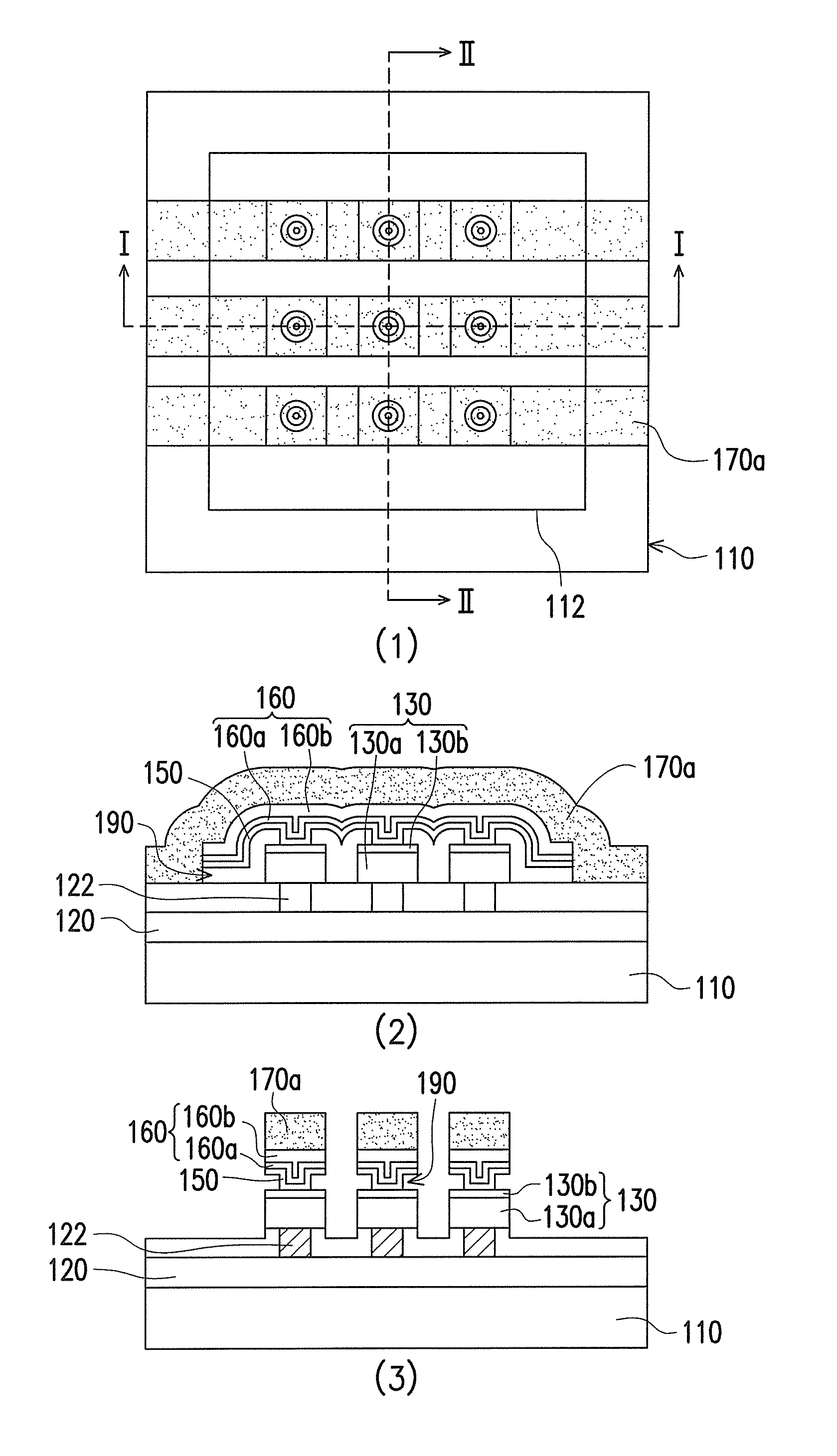
The patent describes a resistive memory device with an air dielectric layer that can operate at high radio frequencies, reduce stray capacitance, and have a high density. The device includes a substrate with conductive channels and bottom electrodes, which are covered by a patterned sacrificial layer. A resistance switching material layer and top electrode layer are sequentially formed on the sacrificial layer, filling the openings. The top electrode, resistance switching material layer, and patterned sacrificial layer outside the active region are removed, and a conductive layer is formed. The conductive layer, top electrode, and resistance switching material layer are then patterned to form interconnections. A reactant is provided to remove the patterned sacrificial layer, leaving an air dielectric layer. The technical effects of this invention include improved performance and reliability of resistive memory devices.

Problems solved by technology

However, during the process of fabricating the resistive memory device, the dielectric layer generates leakage currents due to the process, and the leakage currents damage the electrical characteristics of the resistance switching material layer.
In addition, during the process of fabricating the resistive memory device, charges carried by a plasma which is used for etching or cleaning may also damage the electrical characteristics of the resistance switching material layer.
As a result, an amount of change and a degree of uniformity in the resistance values when the resistive memory device is turned on or turned off are adversely affected.

Method used


Image

  • Resistive memory device with an air gap
  • Resistive memory device with an air gap
  • Resistive memory device with an air gap

Examples


Embodiment Construction

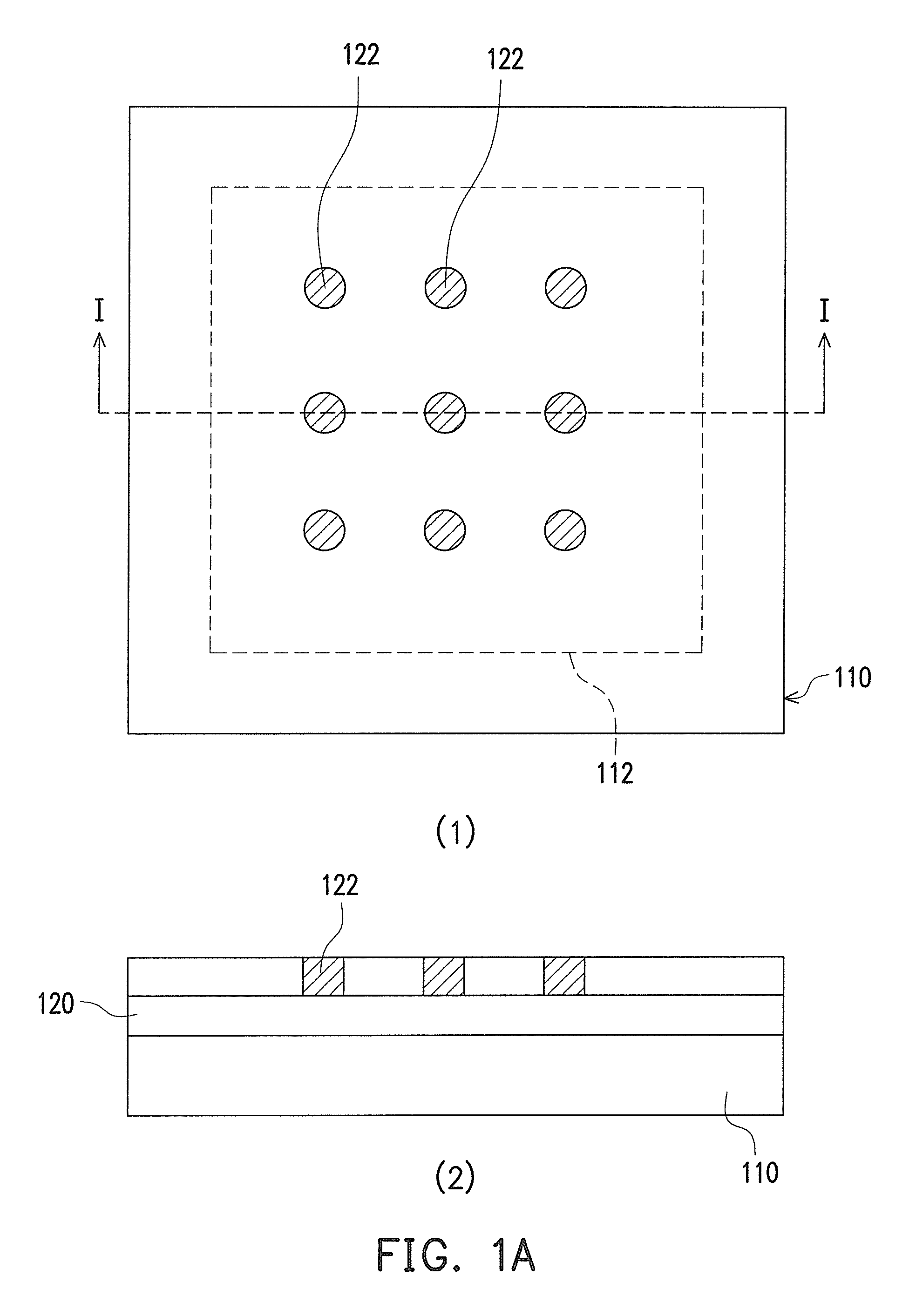
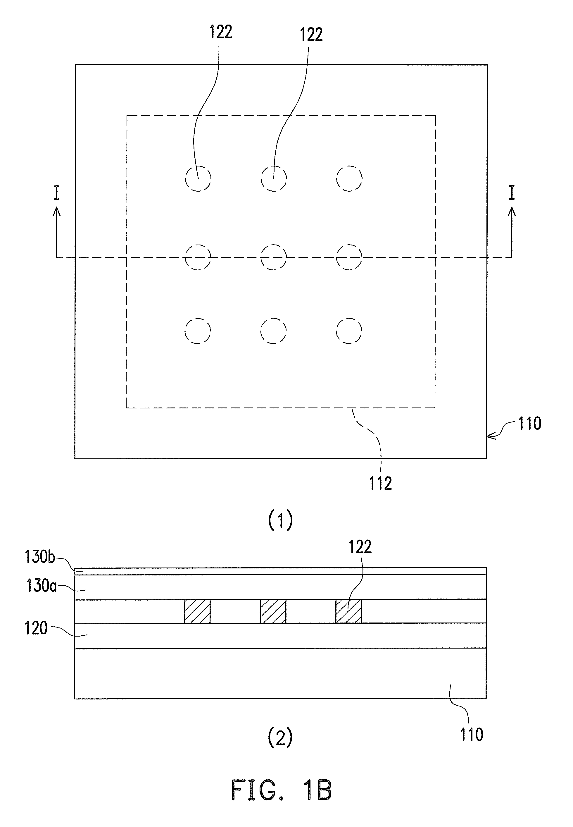
[0016]In one of exemplary embodiments, a resistive memory device fabricating method is provided and may be, but is not limited to being completed by the following steps. A substrate which has an active region is provided. A front end circuit (FEOL CKT) is formed in the active region, and the front end circuit has a plurality of conductive channels arranged as an array. A plurality of bottom electrodes is formed in the action region, and each of the bottom electrodes is disposed to correspond to each of the conductive channels. The patterned sacrificial layer is formed on the substrate and covers the bottom electrodes. The patterned sacrificial layer has a plurality of openings, in which each of the openings is disposed to correspond to each of the bottom electrodes and exposes a part of each of the bottom electrodes.

[0017]A resistance switching material layer and a top electrode layer are sequentially formed on the patterned sacrificial layer, wherein the resistance switching materi...


PUM


Abstract

A resistive memory device and a fabricating method thereof are introduced herein. In resistive memory device, a plurality of bottom electrodes is disposed in active region of a substrate. Each of the bottom electrodes is disposed to correspond to each of the conductive channels; a patterned resistance switching material layer and the patterned top electrode layer are sequentially stacked on the bottom electrodes. An air dielectric layer exists between the patterned resistance switching material layer and the bottom electrodes. A plurality of patterned interconnections is disposed on the patterned top electrode.

Description

CROSS-REFERENCE TO RELATED APPLICATION[0001]This application claims the priority benefit of Taiwan application serial no. 98145665, filed Dec. 29, 2009. The entirety of the above-mentioned patent application is hereby incorporated by reference herein and made a part of specification.BACKGROUND OF THE INVENTION[0002]1. Field of the Invention[0003]The invention is related to a resistive memory device with an air dielectric layer, and a method to fabricate the same.[0004]2. Description of Related Art[0005]As portable products rapidly develop and demands for functions increase, demands in the global memory market are rapidly expanding. In particular, the growth of non-volatile memories (NVM) has drawn the most attention. In order to deal with market changes, big factories and research facilities around the globe have begun development in next generation memory technologies. Among the many types of possible technologies, resistive random access memory (RRAM) is one of highly focused tech...

Claims


Application Information

Patent Timeline
Patent Type & Authority Patents(United States)
IPC IPC(8): H01L47/00H10N80/00
CPCH01L27/24H10B63/00
Inventor CHEN, WEI-SU
Owner IND TECH RES INST
Learn More