
Organic EL display and method of manufacturing the same

a technology of organic el and display, which is applied in the direction of semiconductor devices, semiconductor/solid-state device details, electrical apparatus, etc., can solve the problems of increased tact time and process complication, and achieve the effect of simple process, improved display quality, and excellent electric connection

Active Publication Date: 2012-05-29
JOLED INC
View PDF21 Cites 43 Cited by
  • Summary
  • Abstract
  • Description
  • Claims
  • Application Information

AI Technical Summary

Benefits of technology

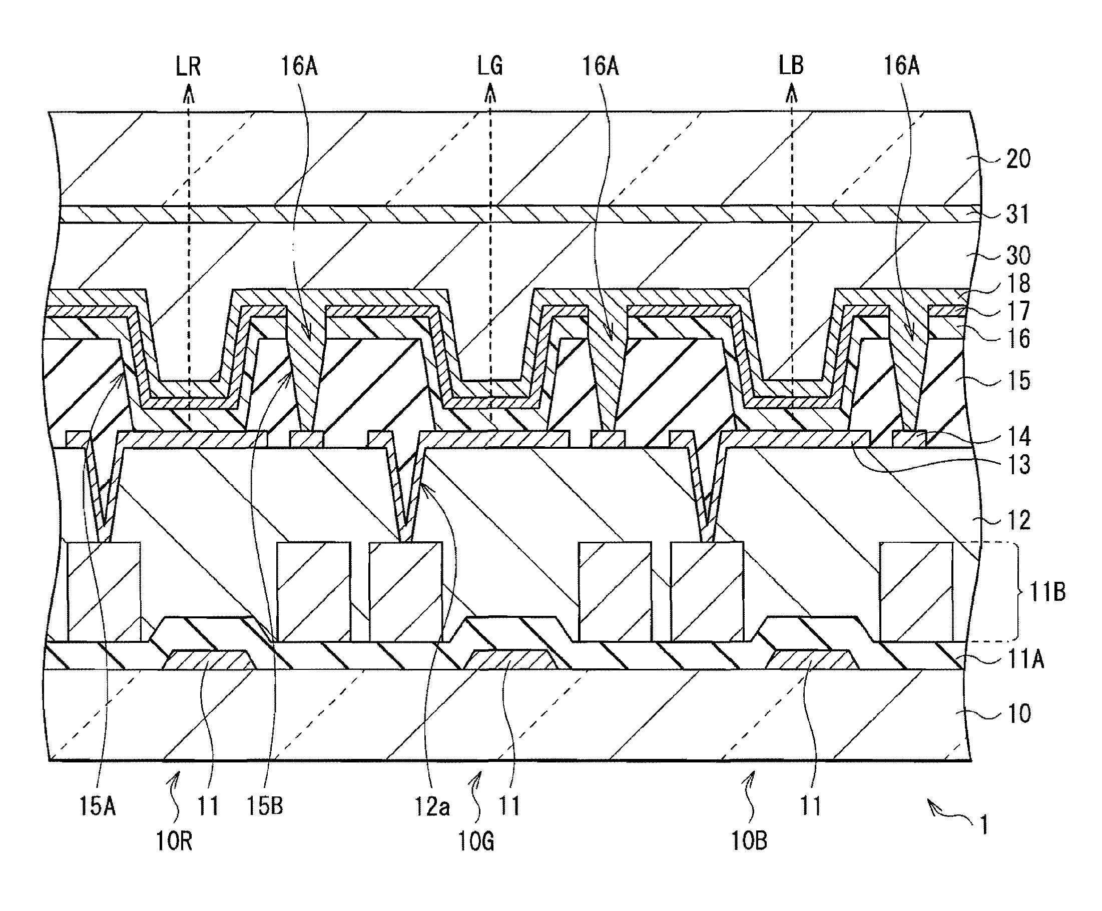
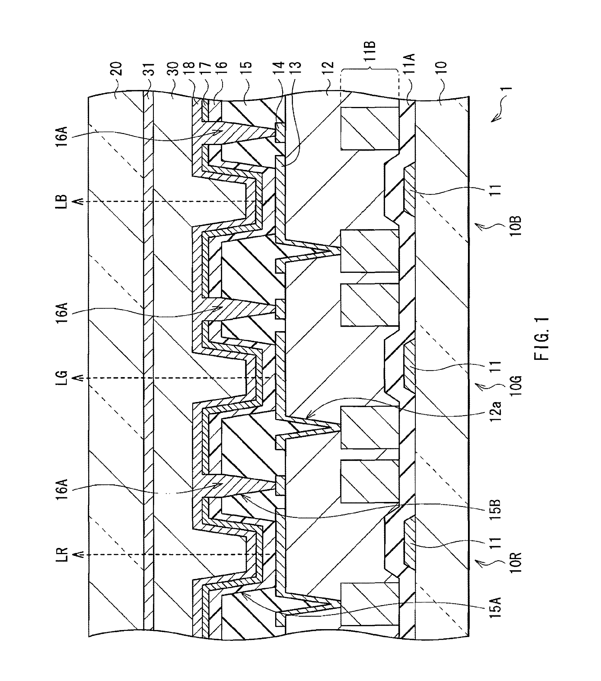
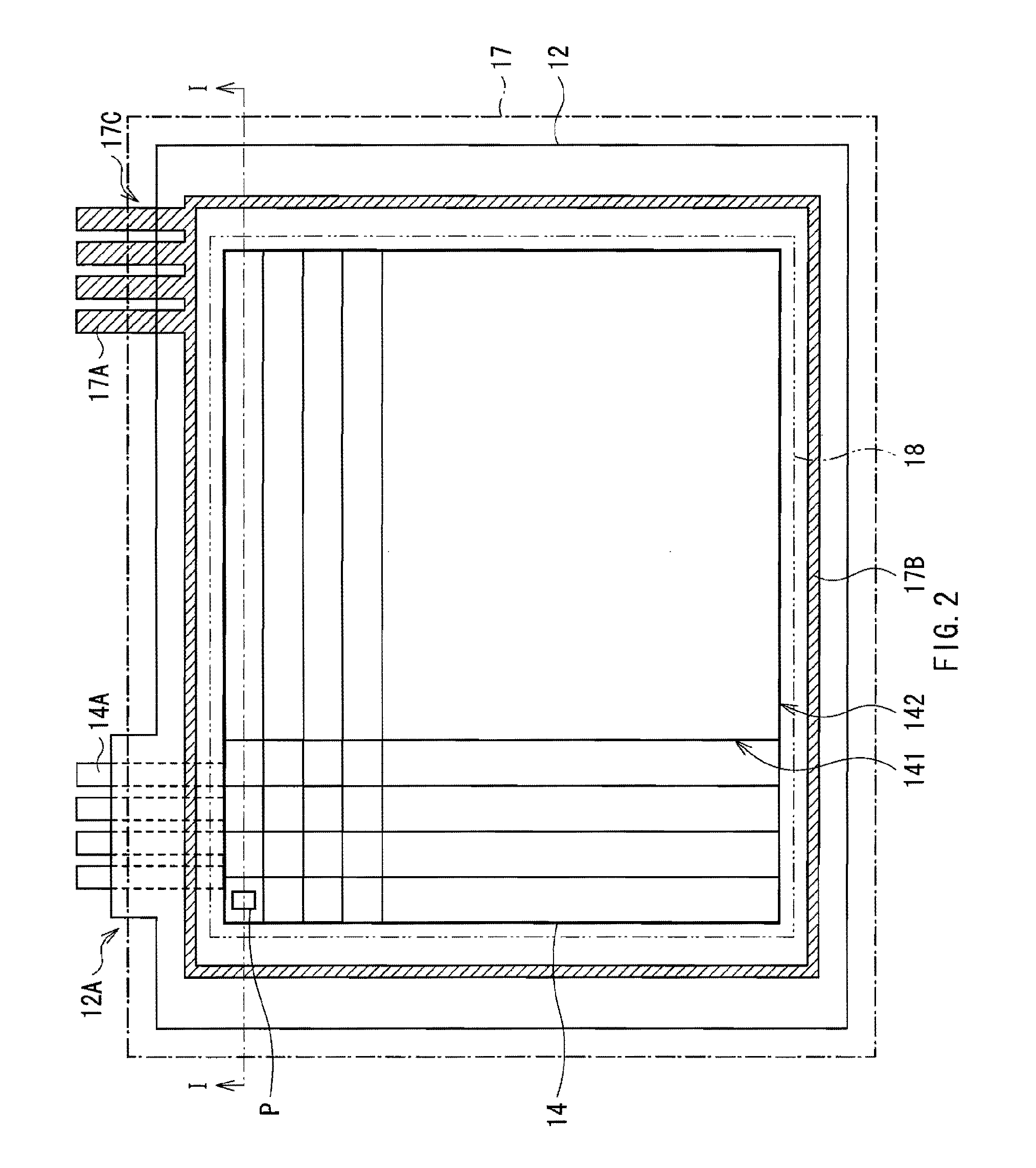
"The patent text describes a method for manufacturing an organic EL display that ensures good electrical connection between the auxiliary wiring and the second electrode without the need for expensive equipment or precise alignment. The method involves forming auxiliary wiring in a peripheral region of each pixel and another auxiliary wiring in a separate formation region. A reverse bias voltage is then applied to the organic layer through the auxiliary wiring and another auxiliary wiring to selectively remove the region on the auxiliary wiring in the organic layer. This removed region is then buryed as a connection hole with the second electrode, ensuring excellent electrical connection. This method simplifies the manufacturing process and reduces the likelihood of voltage drops in the second electrode, resulting in improved display quality."

Problems solved by technology

The irradiation position and the like have to be strictly aligned, so that it causes increase in tact time and complication in processes.

Method used


Image

  • Organic EL display and method of manufacturing the same
  • Organic EL display and method of manufacturing the same
  • Organic EL display and method of manufacturing the same

Examples


application examples

And Modules

[0093]Hereinbelow, modules and application examples of the organic EL displays 1 and 2 explained in the foregoing embodiment will be described. The organic EL displays 1 and 2 is applicable to electronic devices in all of fields for displaying a video signal entered from the outside or generated internally as an image or a video image, such as a television apparatus, a digital still camera, a notebook-sized personal computer, a portable terminal device such as a cellular phone, and a video camera.

Modules

[0094]The organic EL displays 1 and 2 are assembled, for example, as a module illustrated in FIG. 12, in various electronic devices in application examples 1 to 5 and the like which will be described later. The module has, at one side of the drive-side substrate 10, a region 210 exposed from the sealing-side substrate 20. To the region 210, wirings of a signal line drive circuit 120 and a scan line drive circuit 130 which will be described later are extended and external c...

application example 1

[0098]FIG. 15 illustrates the appearance of a television apparatus to which the organic EL displays 1 and 2 of the foregoing embodiment are applied. The television apparatus has, for example, a video image display screen 300 including a front panel 310 and a filter glass 320.

application example 2

[0099]FIGS. 16A and 16B illustrate the appearance of a digital still camera to which the organic EL displays 1 and 2 of the embodiment are applied. The digital still camera has, for example, a light emission unit 410 for flash, a display unit 420, a menu switch 430, and a shutter button 440.


PUM


Abstract

The present invention provides an organic EL display and a method of manufacturing the same capable of assuring excellent electric connection between an auxiliary wiring and a second electrode without using large-scale equipment. The organic EL display includes: a plurality of pixels each having, in order from a substrate side, a first electrode, an organic layer including a light emission layer, and a second electrode; an auxiliary wiring disposed in a periphery region of each of the plurality of pixels and conducted to the second electrode; and another auxiliary wiring disposed apart from the auxiliary wiring at least in a part of outer periphery of a formation region of the auxiliary wiring in a substrate surface.

Description

BACKGROUND OF THE INVENTION[0001]1. Field of the Invention[0002]The present invention relates to an organic EL display provided with an auxiliary wiring and a method of manufacturing the same.[0003]2. Description of the Related Art[0004]In recent years, attention is being paid to an organic EL element using an electro luminescence (EL) phenomenon of an organic material as a light emitting element capable of emitting high-luminance light by low-voltage DC driving. As a method of driving a display device (organic EL display) using the organic EL element, a simple matrix method and an active matrix method are mentioned. In the case where the number of pixels is large, the active matrix method is suitable.[0005]In an organic EL display of the active matrix method, a thin film transistor for driving each pixel (organic EL element), a first electrode connected to the thin film transistor, an organic layer including a light emission layer, and a second electrode are provided in this order ...

Claims


Application Information

Patent Timeline
Patent Type & Authority Patents(United States)
IPC IPC(8): H01L21/02
CPCH01L27/3276H10K59/131H10K59/80522H10K59/1315H01L21/7684H01L2924/13069H10K59/35H10K50/11H10K50/824
Inventor TAKAGI, KAZUNARINAKAMURA, KAZUO
Owner JOLED INC
Learn More