Method of manufacturing electronic component built-in substrate
a technology of built-in substrates and electronic components, which is applied in the direction of final product manufacturing, sustainable manufacturing/processing, fixed capacitor details, etc., can solve the problems of difficult to apply various processes with easy application, and it is extremely difficult to align them mutually with good accuracy, so as to suppress the occurrence of warps and eliminate easily the level difference
- Summary
- Abstract
- Description
- Claims
- Application Information
AI Technical Summary
Benefits of technology
Problems solved by technology
Method used
Image
Examples
first embodiment
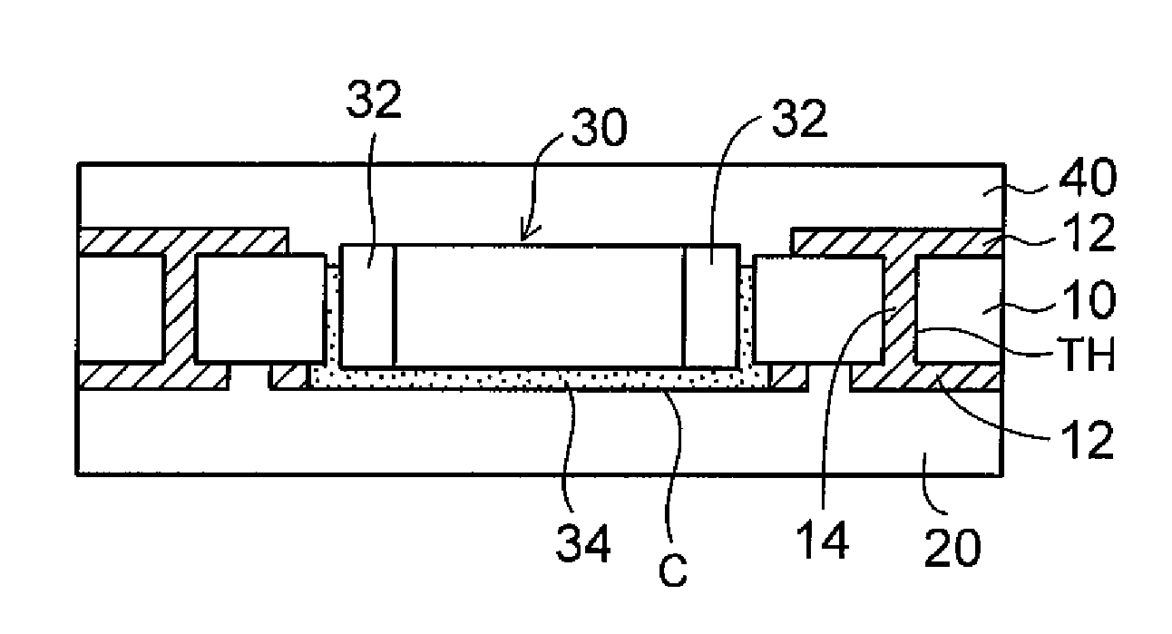
[0041]FIGS. 3A to 3D, FIGS. 4A to 4C, and FIGS. 5A to 5C are sectional views showing a method of manufacturing an electronic component built-in substrate according to a first embodiment of the present invention. In the method of manufacturing the electronic component built-in substrate according to the present embodiment, as shown in FIG. 3A, first, a core substrate 10 on both surface sides of which a first wiring layer 12 is provided respectively is prepared. The core substrate 10 is formed of an epoxy resin into which a glass cloth is contained, or the like, and through holes TH passing through the thickness direction are formed in the core substrate 10. A through electrode 14 is filled in the through holes TH of the core substrate 10 respectively, and the first wiring layers 12 on both surface sides of the core substrate 10 are connected mutually via the through electrodes 14.
[0042]Alternately, a through hole plating layer may be provided on inner surfaces of the through holes TH...
second embodiment
[0083]FIGS. 6A to 6C and FIGS. 7A and 7B are sectional views showing a method of manufacturing an electronic component built-in substrate according to a second embodiment of the present invention.
[0084]In the second embodiment, a semiconductor chip is mounted instead of the capacitor component in the first embodiment. In the second embodiment, detailed explanation about the same steps as those in the first embodiment will be omitted herein.
[0085]In the method of manufacturing the electronic component built-in substrate according to the second embodiment, as shown in FIG. 6A, first, a structure in which the stopper metal layer 12a of the bottom portion of the concave portion C of the mounted body 5 is removed is obtained, like FIG. 3C of the first embodiment.
[0086]Then, as shown in FIG. 6B, a semiconductor chip 50 (LSI chip) having connection terminals 52 (connection pads or connection bumps) is prepared. Then, the semiconductor chip 50 is mounted / bonded on the concave portion C of t...
third embodiment
[0092]FIGS. 8A to 8C are sectional views showing a method of manufacturing an electronic component built-in substrate according to a third embodiment of the present invention.
[0093]In the third embodiment, the semiconductor chip is mounted in a face-up manner in the second embodiment. In the third embodiment, detailed explanation about the same steps as those in the first embodiment will be omitted herein.
[0094]In the method of manufacturing an electronic component built-in substrate according to the third embodiment, as shown in FIG. 8A, in the above step in FIG. 6B of the second embodiment, the semiconductor chip 50 is mounted / bonded on the concave portion C of the mounted body 5 by the adhesive 34 while directing the connection terminals 52 upward (face-up).
[0095]Then, as shown in FIG. 8B, the upper interlayer insulating layer 40 is formed on the semiconductor chip 50 and the core substrate 10 by the similar method to that in the first embodiment.
[0096]Then, as shown in FIG. 8C, ...
PUM
| Property | Measurement | Unit |
|---|---|---|
| depth | aaaaa | aaaaa |
| insulating | aaaaa | aaaaa |
| thickness | aaaaa | aaaaa |
Abstract
Description
Claims
Application Information
 - R&D
- Intellectual Property
- Life Sciences
- Materials
- Tech Scout
- Unparalleled Data Quality
- Higher Quality Content
- 60% Fewer Hallucinations
Browse by: Latest US Patents, China's latest patents, Technical Efficacy Thesaurus, Application Domain, Technology Topic, Popular Technical Reports.
© 2025 PatSnap. All rights reserved.Legal|Privacy policy|Modern Slavery Act Transparency Statement|Sitemap|About US| Contact US: help@patsnap.com


