
Surface acoustic wave resonator having comb electrodes with different overlapping lengths

a surface acoustic wave and comb electrode technology, applied in piezoelectric/electrostrictive/magnetostrictive devices, piezoelectric/electrostriction/magnetostriction machines, electrical apparatus, etc., can solve the problems of ineffective suppression of spurious responses, and inability to suppress spurious responses attributed to resonances. , to achieve the effect of suppressing undesired resonance, preventing spur

Active Publication Date: 2011-12-27
SKYWORKS PANASONIC FILTER SOLUTIONS JAPAN
View PDF30 Cites 1 Cited by
  • Summary
  • Abstract
  • Description
  • Claims
  • Application Information

AI Technical Summary

Benefits of technology

[0018]Since the above structure uses two surface acoustic wave resonators, each having a smaller number of comb electrode fingers, it can suppress undesired resonance in the transverse mode to thereby prevent spurious responses. The structure can also provide a desired value of electrostatic capacitance since it makes use of the first surface acoustic wave resonator and the second surface acoustic wave resonator in parallel connection.
[0019]Accordingly, the present invention can provide the surface acoustic wave resonator having the desired value of electrostatic capacitance while preventing the spurious responses even with a large number of the comb electrode fingers in the aggregate.

Problems solved by technology

In general, however, LiNbO3 substrates degrade the in-band frequency characteristics due to spurious responses caused by resonance in the transverse mode peculiar to them.
Although the apodization is effective to suppress the resonance in the transverse mode of comb electrodes 1 having a small number of electrode fingers as shown in FIG. 10, it is not feasible to suppress spurious responses if comb electrodes 1 have a large number of electrode fingers as is the case of another conventional surface acoustic wave resonator shown in FIG. 11 since it bears a high amplitude of excitation in the transverse mode.
Although adoption of this structure can help widen a bandwidth and improve a temperature characteristic of the surface acoustic wave resonator, it is not effective to suppress the spurious responses attributed to the resonance in the transverse mode when the number of electrode fingers of the comb electrodes is increased to about 300, for instance.
However, this gives rise to a problem that spurious responses are liable to occur when the number of electrode fingers of comb electrodes 1 is increased to obtain a large capacitance.[Patent Document 1] Japanese Patent Unexamined Publication, No. 1990-11012[Patent Document 2] Japanese Patent Unexamined Publication, No. 1994-85602

Method used


Image

  • Surface acoustic wave resonator having comb electrodes with different overlapping lengths
  • Surface acoustic wave resonator having comb electrodes with different overlapping lengths
  • Surface acoustic wave resonator having comb electrodes with different overlapping lengths

Examples


first exemplary embodiment

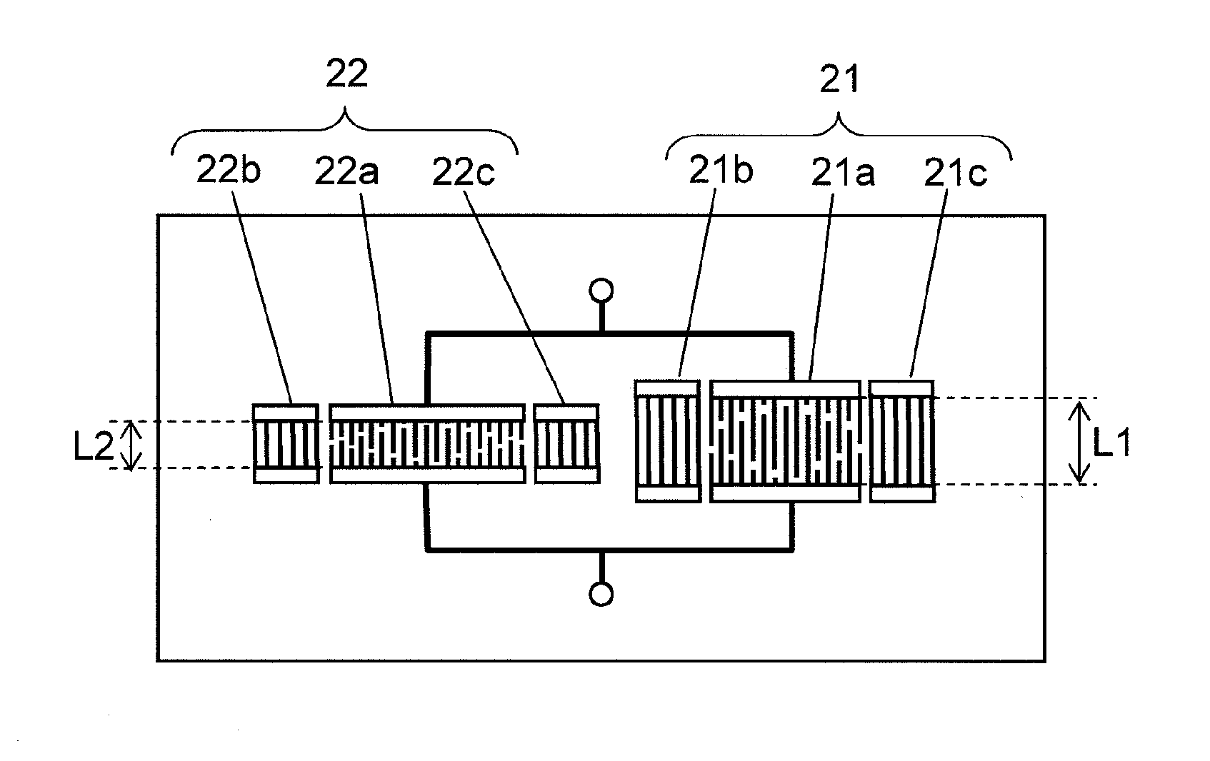
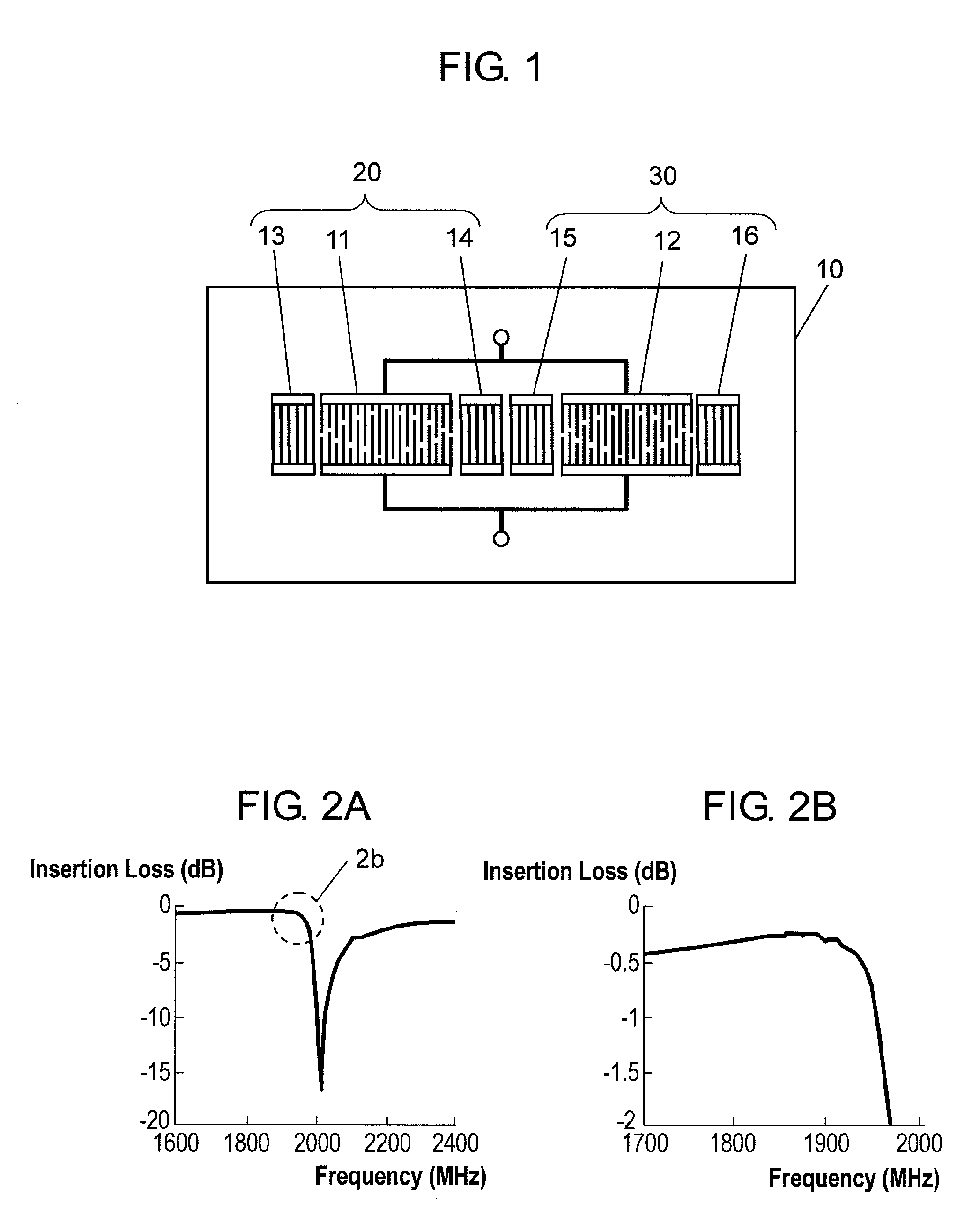
[0045]FIG. 1 shows a plan view of a surface acoustic wave resonator according to the first exemplary embodiment of the present invention.

[0046]As shown in FIG. 1, the surface acoustic wave resonator of the first exemplary embodiment includes piezoelectric substrate 10, first surface acoustic wave resonator 20 having comb electrodes 11 provided on piezoelectric substrate 10, and second surface acoustic wave resonator 30 having comb electrodes 12 provided on piezoelectric substrate 10. First surface acoustic wave resonator 20 and second surface acoustic wave resonator 30 have an apodized configuration as shown in FIG. 1, and they are connected in parallel.

[0047]In other words, the surface acoustic wave resonator shown in the first exemplary embodiment is comprised of comb electrodes 11 and 12, and reflectors 13, 14, 15 and 16, all formed on piezoelectric substrate 10 made of a material such as LiNbO3. Reflectors 13 and 14 are disposed in close proximity to both sides of comb electrode...

second exemplary embodiment

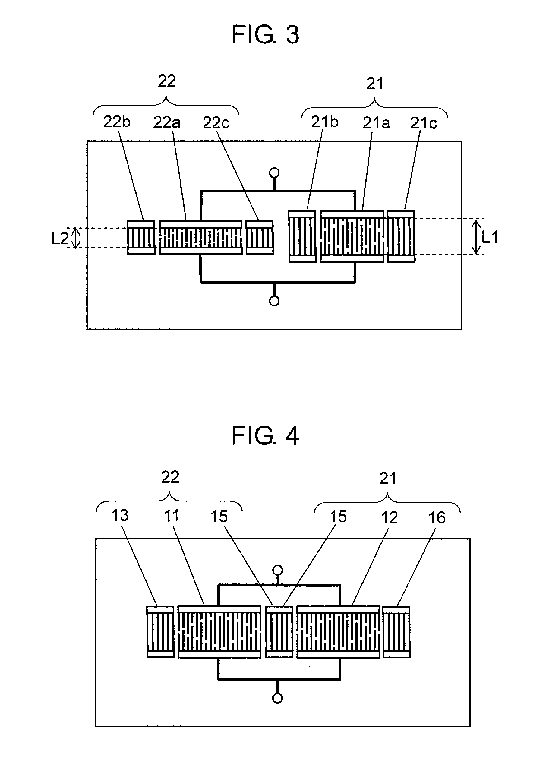
[0058]FIG. 4 shows a plan view of a surface acoustic wave resonator according to the second exemplary embodiment of the present invention.

[0059]The surface acoustic wave resonator of this invention has a structure, in which either reflector 14 or reflector 15 between comb electrodes 11 and 12 shown in FIG. 1 is eliminated, so that the remaining element designated as reflector 15 is used to serve commonly for both comb electrodes 11 and 12. In other words, first surface acoustic wave resonator 21 and second surface acoustic wave resonator 22 share a function of reflector 15 provided between them. This structure allows further reduction in size of the surface acoustic wave resonator as compared to the one shown in FIG. 1 of the first exemplary embodiment.

[0060]FIG. 5A shows a pass-band characteristic of this surface acoustic wave resonator, and FIG. 5B shows a part of the pass-band characteristic, wherein domain 5b encircled by a dotted line in FIG. 5A is enlarged.

[0061]As is apparent...

third exemplary embodiment

[0062]FIG. 6 shows a plan view of a surface acoustic wave resonator according to the third exemplary embodiment of the present invention.

[0063]The surface acoustic wave resonator of this invention has a structure, in which both reflectors 14 and 15 located between comb electrodes 11 and 12 shown in FIG. 1 are eliminated, and comb electrodes 11 and 12 are disposed close to each other. In other words, first surface acoustic wave resonator 21 and second surface acoustic wave resonator 22 share functions of reflectors 13 and 16 that sandwich comb electrodes 11 and 12 between them. This structure allows even further reduction in size of the surface acoustic wave resonator as compared to those discussed in the first and the second exemplary embodiments.

[0064]FIG. 7A shows a pass-band characteristic of this surface acoustic wave resonator, and FIG. 7B shows a part of the pass-band characteristic, wherein domain 7b encircled by a dotted line in FIG. 7A is enlarged.

[0065]As is apparent from ...


PUM


Abstract

A surface acoustic wave resonator includes a piezoelectric substrate, a first surface acoustic wave resonator having a comb electrode provided on the piezoelectric substrate, and a second surface acoustic wave resonator having a comb electrode provided on the piezoelectric substrate. The first surface acoustic wave resonator and the second surface acoustic wave resonator are apodized and connected in parallel.

Description

BACKGROUND OF THE INVENTION[0001]1. Technical Field[0002]The present invention relates to surface acoustic wave resonators used for telecommunications devices of high frequency bands such as mobile phones.[0003]2. Background Art[0004]There is a rising demand in recent years for surface acoustic wave resonators having filtering characteristics over wide frequency bands. In order to produce wide frequency band filters, it is generally necessary to choose substrates made of a material having a large electromechanical coupling coefficient.[0005]LiNbO3 substrates used conventionally are effective for widening frequency bands of the surface acoustic wave filters because of the large electromechanical coupling coefficient. In general, however, LiNbO3 substrates degrade the in-band frequency characteristics due to spurious responses caused by resonance in the transverse mode peculiar to them.[0006]FIG. 8 shows a plan view of a conventional surface acoustic wave resonator provided with norma...

Claims


Application Information

Patent Timeline
Patent Type & Authority Patents(United States)
IPC IPC(8): H03H9/25H03H9/145
CPCH03H9/02559H03H9/25H03H9/1452
Inventor HAMAOKA, YOSUKENAKANISHI, HIDEKAZUNAKAMURA, HIROYUKIGOTO, REI
Owner SKYWORKS PANASONIC FILTER SOLUTIONS JAPAN
Learn More