
Linearity improvements of semiconductor substrate based radio frequency devices

a radio frequency device and semiconductor substrate technology, applied in semiconductor devices, semiconductor/solid-state device details, electrical devices, etc., can solve the problems of non-linear capacitance, non-linear conductance, non-linear capacitance, affecting the rf interaction between the silicon substrate and other layers, and achieving the effect of effectively immobilizing the surface conduction layer, preventing capacitance and inductance changes, and significantly reducing harmonic distortion of rf signals

Active Publication Date: 2011-12-13
QORVO US INC
View PDF6 Cites 94 Cited by
  • Summary
  • Abstract
  • Description
  • Claims
  • Application Information

AI Technical Summary

Benefits of technology

The present invention relates to using a trap-rich layer to immobilize a surface conduction layer at RF frequencies, which can reduce harmonic distortion of RF signals. This is achieved by trapping carriers from the surface conduction layer and preventing capacitance and inductance changes due to RF signals. The use of a trap-rich layer can be in combination with a metallization layer or an insulator layer, and can be applied to different substrates such as Silicon or Gallium Arsenide. The invention provides a way to improve the performance and reliability of RF devices and systems.

Problems solved by technology

However, Silicon has certain characteristics that may produce undesirable behavior in some RF applications.
RF signals traversing above the surface of the Silicon substrate may modulate the surface conduction layer, which may cause non-linear capacitance, non-linear conductance, or both affecting RF interactions between the Silicon substrate and other layers.
The non-linear characteristics may introduce harmonic distortion in the RF signals, which may exceed allowable limits.
One technique for reducing the impact of the non-linear characteristics is to incorporate a conductive shielding layer between the surface of the Silicon substrate and other layers handling RF signals; however, the conductive shielding layer may increase complexity and signal loss.

Method used


Image

  • Linearity improvements of semiconductor substrate based radio frequency devices
  • Linearity improvements of semiconductor substrate based radio frequency devices
  • Linearity improvements of semiconductor substrate based radio frequency devices

Examples


Embodiment Construction

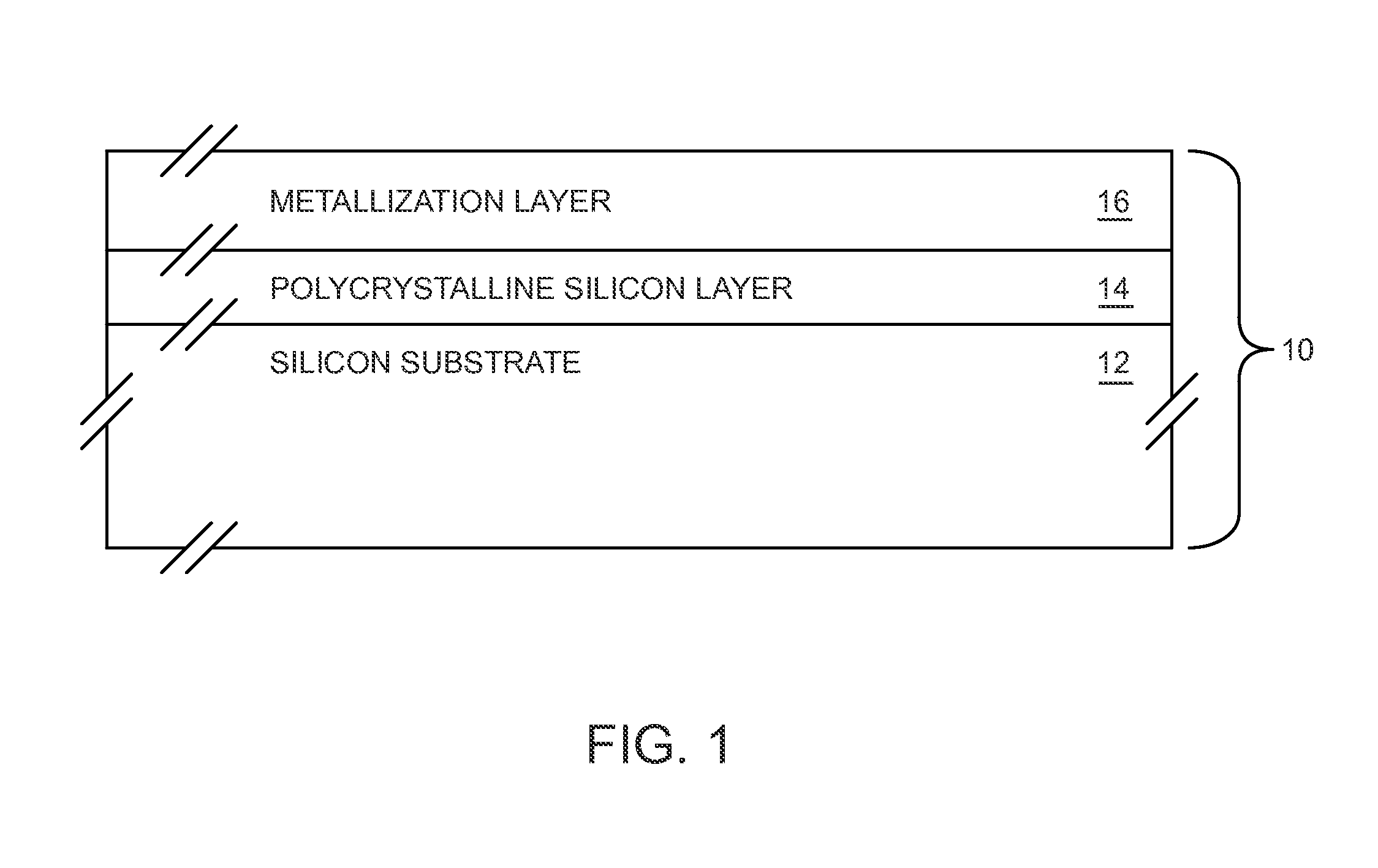
[0005]The present invention relates to using a trap-rich layer, such as a polycrystalline Silicon layer, over a semiconductor substrate to substantially immobilize a surface conduction layer at the surface of the semiconductor substrate at radio frequency (RF) frequencies. The trap-rich layer may have a high density of traps that trap carriers from the surface conduction layer. The average release time from the traps may be longer than the period of any present RF signals, thereby effectively immobilizing the surface conduction layer, which may substantially prevent capacitance and inductance changes due to the RF signals. Therefore, harmonic distortion of the RF signals may be significantly reduced or eliminated. The semiconductor substrate may be a Silicon substrate, a Gallium Arsenide substrate, or another substrate.

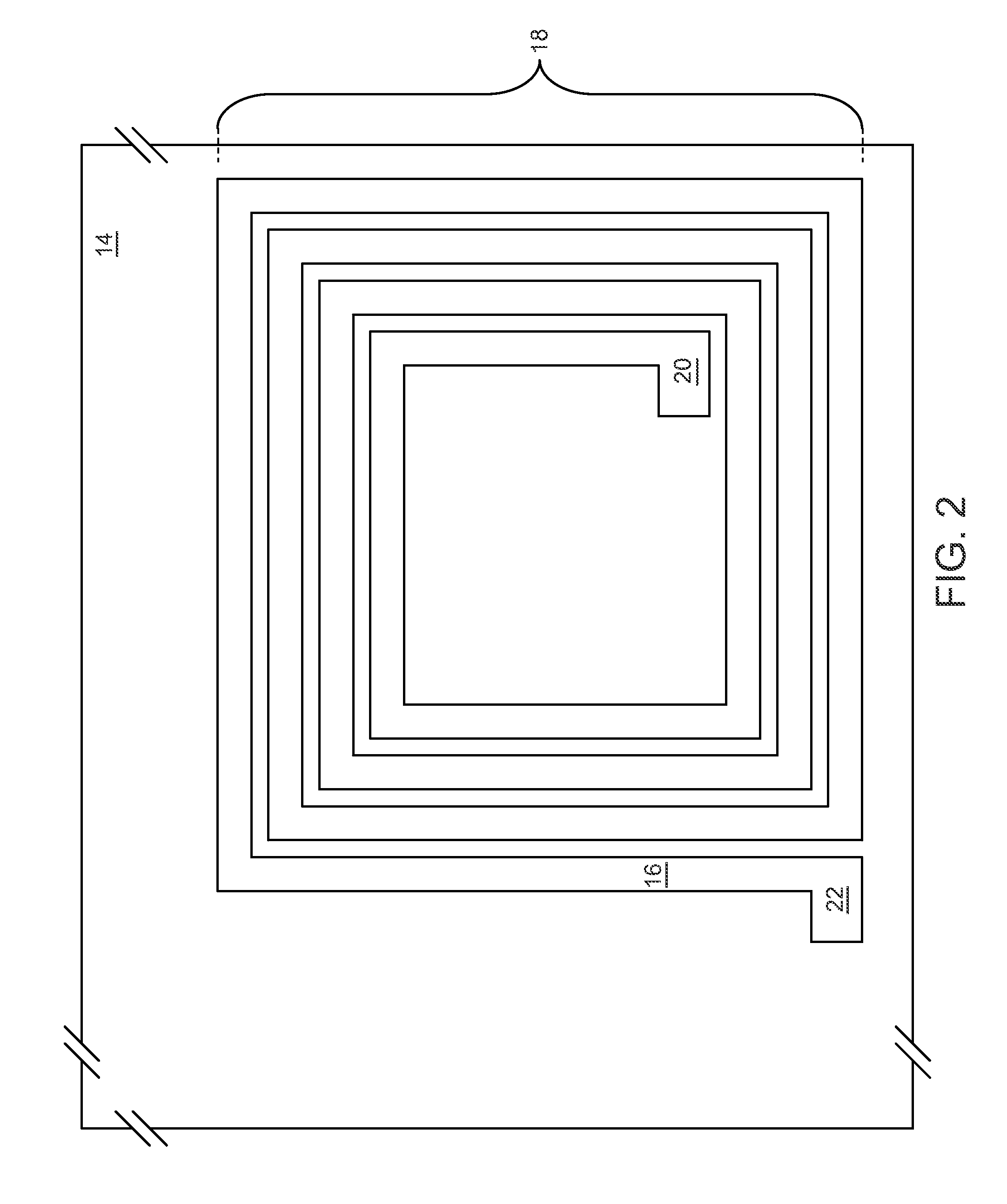
[0006]In one embodiment of the present invention, a metallization layer may be applied directly to the trap-rich layer. Other embodiments of the present invention may...


PUM


Abstract

The present invention relates to using a trap-rich layer, such as a polycrystalline Silicon layer, over a semiconductor substrate to substantially immobilize a surface conduction layer at the surface of the semiconductor substrate at radio frequency (RF) frequencies. The trap-rich layer may have a high density of traps that trap carriers from the surface conduction layer. The average release time from the traps may be longer than the period of any present RF signals, thereby effectively immobilizing the surface conduction layer, which may substantially prevent capacitance and inductance changes due to the RF signals. Therefore, harmonic distortion of the RF signals may be significantly reduced or eliminated. The semiconductor substrate may be a Silicon substrate, a Gallium Arsenide substrate, or another substrate.

Description

[0001]This application is a Divisional of U.S. patent application Ser. No. 12 / 254,499, filed Oct. 20, 2008, now U.S. Pat. No. 7,868,419, which claims the benefit of U.S. Provisional Patent Application 60 / 980,914, filed Oct. 18, 2007, the disclosures of which are hereby incorporated herein by reference in their entireties.FIELD OF THE INVENTION[0002]Embodiments of the present invention relate to Silicon substrates used to manufacture semiconductor devices, which may be used in radio frequency (RF) communications systems.BACKGROUND OF THE INVENTION[0003]Silicon substrates are widely used in the manufacture of semiconductor devices. Low cost and highly evolved manufacturing techniques make Silicon a preferred material in many applications, when compared with other semiconductor materials. High resistivity Silicon substrates may be used in radio frequency (RF) devices. If the period of an RF signal is shorter than a majority carrier relaxation time, then the majority carriers in a Silic...

Claims


Application Information

Patent Timeline
Patent Type & Authority Patents(United States)
IPC IPC(8): H01L29/00
CPCH01L23/645H01L23/66H01L23/5227H01L23/552H01L2924/0002H01L2924/00
Inventor KERR, DANIEL CHARLESMCKAY, THOMAS GREGORYCARROLL, MICHAELGERING, JOSEPH M.
Owner QORVO US INC
Learn More