Transflective liquid crystal display panel with integrated switch element and color filter layer on a substrate
a technology of liquid crystal display panel and color filter layer, which is applied in non-linear optics, instruments, optics, etc., can solve the problems of inability to rework the color filter layer on the array substrate, difficulty in removing the color filter layer from the array substrate, and light leakage phenomenon, so as to increase the intensity of reflected light and the reflectivity of the display panel. , the effect of reducing the misalignment between two substrates
- Summary
- Abstract
- Description
- Claims
- Application Information
AI Technical Summary
Benefits of technology
Problems solved by technology
Method used
Image
Examples
first embodiment
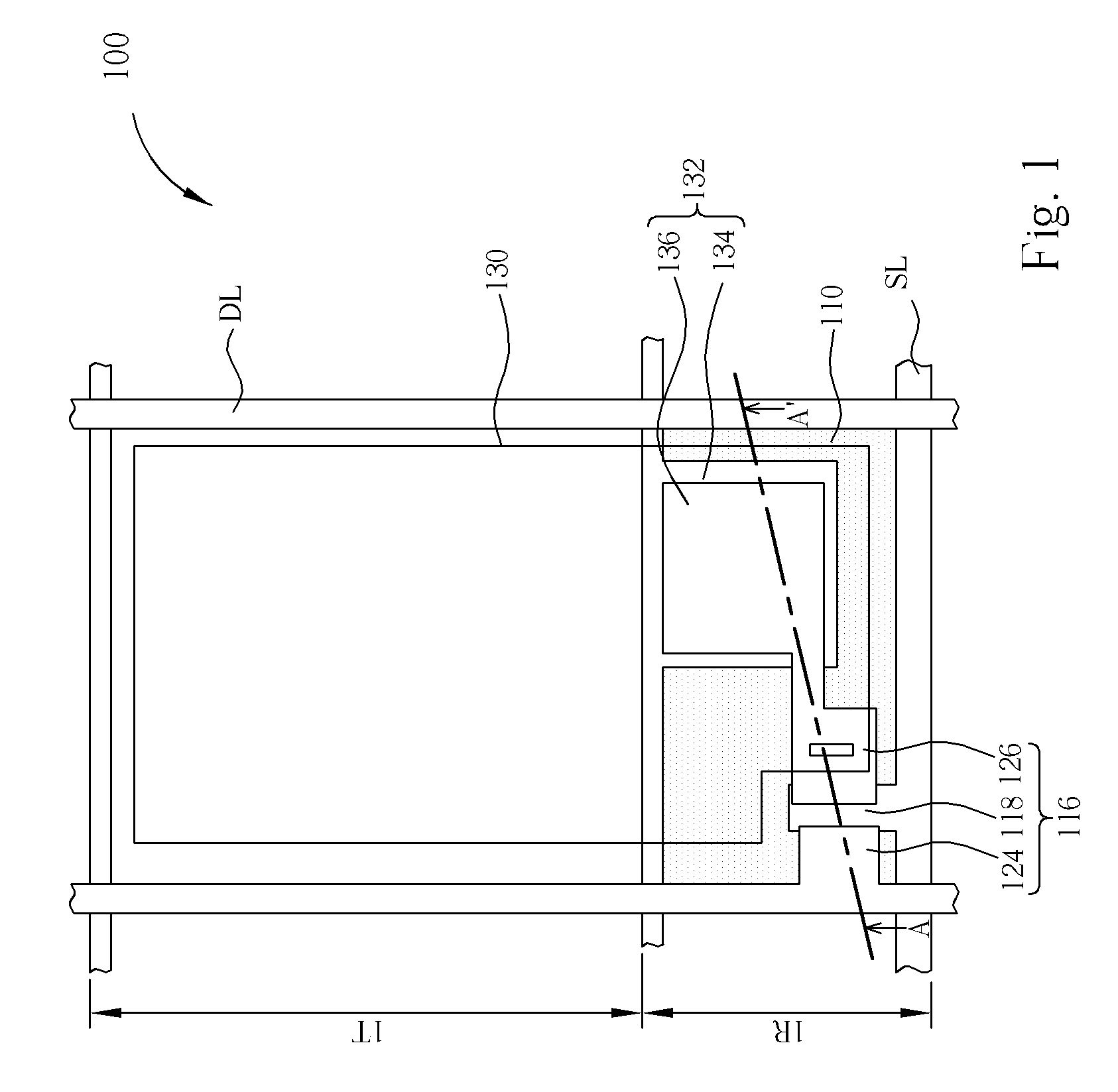
[0026]Referring to FIG. 1 and FIG. 2, FIG. 1 illustrates a top-view of a pixel 100 of a transflective liquid crystal display panel according to the first embodiment of the present invention. FIG. 2 illustrates a cross-section along the line A-A′ shown in FIG. 1. The pixel 100 includes a bottom substrate 102 (such as first substrate), a top substrate 103 (such as second substrate), and a liquid crystal layer 104. The top substrate 103 includes a transparent substrate 105 and a common electrode 106, in which the top substrate 103 can be a vertical alignment liquid crystal display panel or a multi-domain vertical alignment liquid crystal display (MVA-LCD) panel. Instead of being disposed on the transparent substrate 105, the common electrode 106 can also be disposed on the bottom substrate 102 to form an in-plane switching liquid crystal display (IPS-LCD). The bottom substrate 102 includes a transparent substrate 108 and a color filter layer 112 disposed on the transparent substrate 10...
second embodiment
[0030]FIG. 3 illustrates a pixel 300 of a transflective liquid crystal display panel according to the second embodiment of the present invention. The second embodiment is structurally similar to the first embodiment described above. However, in this embodiment, the first reflective layer 310 is not only disposed below the interval between the scan line SL and the pixel electrode 130, but also below the interval between the data line DL and the pixel electrode 130 for reflecting ambient light. Additionally, the first reflective layer 310 can also be disposed either below the interval between the scan line and the pixel electrode 130 or below the interval between the data line and the pixel electrode 130. In other words, the first reflective layer 310 is disposed below at least one of the interval between the scan line SL and the pixel electrode 130, and the interval between the data line DL and the pixel electrode 130.
[0031]In this embodiment, a first reflective layer 310 is disposed...
third embodiment
[0032]FIG. 4 illustrates a cross-section of a pixel 400 of a transflective liquid crystal display panel according to the third embodiment of the present invention. The third embodiment is structurally similar to the first embodiment. However, in this embodiment, the first reflective layer 410 includes a rough and uneven surface, such as a waved surface, such that the waved surface increases the reflectance of ambient lights and enhances the uniformity of light distribution. Preferably, the fabrication of the waved surface of the first reflective layer 410 can be achieved by first forming an insulating layer 402 between the transparent substrate 108 and the color filter layer 112. Thereafter, a series of exposure, development, and etching processes is performed to form a waved surface on a portion of the insulating layer 402 surface, and the first reflective layer 410 is disposed on the waved surface of the insulating layer 402. Alternatively, a series of exposure, development, and e...
PUM
| Property | Measurement | Unit |
|---|---|---|
| depth | aaaaa | aaaaa |
| depth | aaaaa | aaaaa |
| transparent | aaaaa | aaaaa |
Abstract
Description
Claims
Application Information
 - R&D
- Intellectual Property
- Life Sciences
- Materials
- Tech Scout
- Unparalleled Data Quality
- Higher Quality Content
- 60% Fewer Hallucinations
Browse by: Latest US Patents, China's latest patents, Technical Efficacy Thesaurus, Application Domain, Technology Topic, Popular Technical Reports.
© 2025 PatSnap. All rights reserved.Legal|Privacy policy|Modern Slavery Act Transparency Statement|Sitemap|About US| Contact US: help@patsnap.com


